M.A. Kemp#, C. Burkhart, M.N. Nguyen, SLAC, Menlo Park, CA, D.E. Anderson, ORNL, Oak Ridge, TN
Abstract
The 1-MW High Voltage Converter Modulators [1] have operated in excess of 250,000 hours at the Spallation Neutron Source. Increased demands on the accelerator performance require increased modulator reliability. An effort is underway at SLAC National Accelerator Laboratory to redesign the modulator H-bridge switch plate with the goals of increasing reliability and performance [2]. The major difference between the SLAC design and the existing design is the use of press-pack IGBTs. Compared to other packaging options, these IGBTs have been shown to have increased performance in pulsed-power applications, have increased cooling capability, and do not fragment and disassemble during a fault event. An overview of the SLAC switch plate redesign is presented. Design steps including electrical modeling of the modulator and H-bridge, development of an integrated IGBT clamping mechanism, and fault tests are discussed. Experimental results will be presented comparing electrical performance of the SLAC switch plate to the existing switchplate under normal and fault conditions.
System Description
A simplified diagram of the power flow for the SNS HVCMs is shown in Figure 1. There are various configurations of the modulators at the SNS. The IGBT switching voltage is up to 2200V, with peak currents up to 2500A. The switching frequency is 20 kHz. The peak power to the load is up to 15 MW and average power is up to 1 MW.
Mechanical Design
Press-pack IGBTs were chosen to replace the flat-pack IGBTs in the existing modulator. Press-pack IGBTs have several advantages, including:
- It was desired to raise the voltage margin from 3.3 kV to 4.5 kV. At the time of the design, 4.5kV, 1.2 kA IGBTs were only readily available in press-pack packaging.
- Press-pack IGBTs can be cooled on both sides of the die. This aids in heat removal.
- Press-pack IGBTs have been shown to have increased reliability in pulsed-power applications [3].
- In a fault event, the press-pack package will not fragment. IGBT fragmentation in the existing switch plate has in some cases resulted in collateral damage.
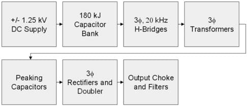
Figure 1: SNS HVCM power flow diagram.
Because of the packaging differences between the flatpack and press-pack IGBTs, a redesign of the mounting hardware for the devices was necessary. The existing and SLAC-designed switch plates are shown in Figures 2 and 3 respectively. During the redesign, care was taken to minimize the altered hardware on the switch plate.
The two largest challenges with redesigning the switch plate included clamping the press-pack packages and minimizing the effects of lead inductance. The press-pack devices require a 30 kN (3700 lbf.) force applied evenly across the electrode faces. In press-pack packages, the clamp force is typically applied to the center of a large force spreader. This is not easily achievable with the SNS switch plate because of insufficient space.

Figure 2: Existing H-bridge switch plate on SLAC test stand.
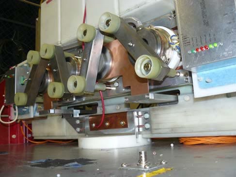
Figure 3: SLAC designed press-pack switch plate.
After the clamps were designed and built, a study was conducted using Fuji Prescale film and varying sizes of shims placed under the heat sinks [4]. A pressure profile resulting from this study is shown in Figure 4. As shown, the pressure is azimuthally symmetric around the surface of the device. To verify the magnitude of the force applied to the device, the calibrated pressure profile was spatially integrated. For all devices, the measured force falls within manufacturer’s specifications.
Lead inductance plays a roll in both the transient characteristics during turn-on and turn-off (such as overshoot) as well as device performance during a fault condition. In general, high inductance in the commutation path will lead to a larger overshoot. However, in some conditions large inductance can be beneficial in limiting the rate of rise of current during a fault condition. During design, finite element simulations were performed on the switch plate geometries. It was found that the effective inductance in the nominal conduction path was increased slightly with the press-pack switch plate. However, the inductance in the shoot-through path was increased by a large amount [5].
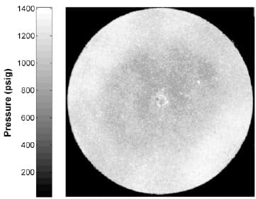
Figure 4: Measured pressure profile on top surface of press-pack IGBT.
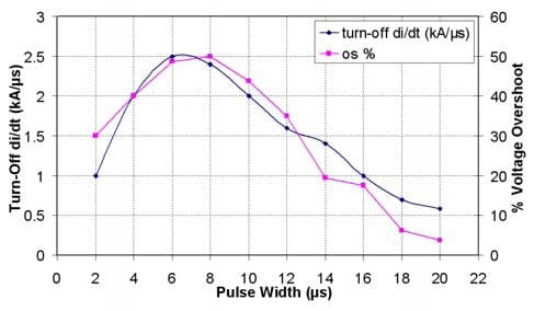
Figure 5: Measured turn-ff di/dt for the press-pack IGBT at a capacitor charge of +/- 400V. The di/dt magnitude correlates with the percentage voltage overshoot.
Switching Waveforms
Shown in Figure 5 is one effect of lead inductance. It was found that for shorter pulses, the collector current turn-off was much quicker. This is consistent with the characteristic of drift regions in power IGBTs. As the device turns on, charge is injected into the drift region, gradually reducing the IGBT resistance. A drift region full of charge turns off slower than a drift region which is not full of charge [6]. Therefore, short pulses result in an IGBT that quickly snaps off. Due to the inductance in the commutation path, the high di/dt increases the voltage overshoot. Proper sizing of the gate turn-off resistance partially mitigates the effect by increasing the turn-off time.
A second characteristic of power IGBTs is a long current tail on turn-off. This has the undesirable effect of increasing turn-off losses. A comparison between two different IGBTs is shown in Figures 6 and 7. The existing IGBT, CM1200HB66H, has a smaller tail than the presspack IGBT, T1200EA45E. This is consistent with the fact that a higher-voltage device typically has a larger drift region. However, by tailoring of the drift region characteristics, it is possible to minimize switching losses at the expense of increased conduction losses. Identification of vendors to supply devices tailored to the SNS application is ongoing. One effect of increased losses, device heating, may be partially mitigated by the improved avenues for heat removal in the press-pack package.
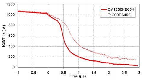
Figure 6: Comparison of the turn-off Ic waveforms for two different IGBTs.
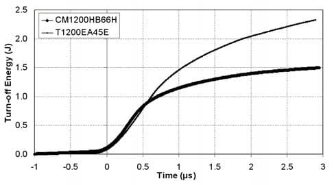
Figure 7: Comparison of the turn-off energy waveforms
Fault Tests
On the SLAC single-phase test stand, several fault tests were performed on both the existing switch plate as well as the press-pack switch plate. The goal was to test the performance of the SLAC-designed gate driver on each of the switch plates [7]. Fault tests included a transformer primary arc-down as well as a forced transformer saturation. In the event of either of these faults, the gate drive should quickly detect the fault and shut-down the IGBT before the current rises to an unacceptable level.
Both switch plate versions survived the fault tests. The newly-developed gate drive was able to quickly detect and control the IGBTs during the faults. However, it was noted that, during an arc-down test, the press-pack switch plate had around a 25% lower dic/dt from the time of arc inception to IGBT commutation [5]. Low di/dt is necessary to retain control of the IGBT via the gate. Therefore, during more stressful fault scenarios, the presspack switch plate may prove advantageous. The lower di/dt is attributed to higher inductance in the shootthrough path as well as differences between IGBTs. It is also noted that at no time during the testing and development of the press pack switch plate did the IGBTs fragment.
Ongoing Work
The press-pack switch plate has been designed, manufactured, and tested to peak power. There are several tasks that are still ongoing:
- The effects of IGBT turn-off at low current are being studied. There are varying modulator “tunes” at the SNS which have different switching characteristics. The switch plate is expected to be able to be implemented in any tune.
- Full average power tests are underway. Switching loss and performance will be compared to the existing devices.
- With the press-pack mounting hardware designed and implemented, it is possible to easily compare devices from various manufacturers. Different vendors are being explored for potential application with the switch plate.
References
- W. A. Reass, et al., “Design, Status, and First Operations of the Spallation Neutron Source Polyphase Resonant converter Modulator System”, PAC, May 2003, p. 553 (2003).
- M.A. Kemp, C. Burkhart, Minh N. Nguyen, D.E. Anderson, “Next Generation IGBT Switch Plate Development for the SNS High Voltage Converter Modulator,” LINAC’08, Victoria, October 2008, THP096, p. 997 (2008); https://www.JACoW.org.
- F. Wakeman, et al., “Press-pack IGBTs, Semiconductor Switches for Pulse Power,” in proc. IEEE Pulsed Power Plasma Science Conference 2001, p.1051.
- Fuji Prescale Film, Fijifilm NDT, Hanover Park, IL.
- M.A. Kemp, C. Burkhart, M.N. Nguyen, D.E. Anderson, “Redesign of the SNS Modulator HBridge for Utilization of Press-Pack IGBTs,” submitted to IEEE Transactions on Dielectrics and Electrical Insulation.
- N. Mohan, Power Electronics, Hoboken: 2003.
- M.N. Nguyen, C. Burkhart, M.A. Kemp, D.E. Anderson, “Advanced Gate Drive for the SNS High Voltage Converter Modulator,” these proceedings.


