NWangler¹, L Gutzweiler¹, K Kalkandjiev¹, C Müller², F Mayenfels³, H Reinecke²,4, R Zengerle1,4,5 and N Paust4
¹ Laboratory for MEMS Applications, Department of Microsystems Engineering—IMTEK, University of Freiburg, Germany
² Laboratory for Process Technology, Department of Microsystems Engineering—IMTEK, University of Freiburg, Germany
³ Department of Pharmaceutical Technology and Biopharmacy, University of Freiburg, Germany
4 HSG-IMIT, Wilhelm-Schickard-Straße 10, 78052 Villingen-Schwenningen, Germany
5 BIOSS—Centre for Biological Signalling Studies, University of Freiburg, Germany
6 DMEM—Dulbecco’s Modified Eagle Medium, order no 11880028, Invitrogen GmbH, Darmstadt, Germany.
7 Cell TiterGlo, Luminescent Viability Assay (Promega Corp.,Madison, WI, USA).
Abstract
We demonstrate the use of photosensitive epoxy laminate TMMF S2045 for the fabrication and sealing of tapered microfluidic channels. The 45 µm thick resist enables the fabrication of shallow sealed cavities featuring extreme aspect ratios of less than 1:40 (h = 45 µm, w = 2000 µm). It also provides high resolution and enables minimum feature sizes of 10 µm. For the fabrication of free-standing structures, an aspect ratio of up to 7:1 was achieved. The dry-film photoresist can be applied easily by lamination onto structured substrates. The total thickness variation of the resist across a 100 mm wafer was determined to be less than ±0.6 µm. Process parameters for the fabrication and sealing of various micro-channels are discussed and optimized in this paper. The main focus was to minimize thermal impact during lamination, soft-bake, exposure and post–exposure bake, which could lead to lid sagging or channel clogging due to liquefaction of uncured resist. We tested TMMF according to ISO 10995-5 and found it to be non-cytotoxic, enabling its use for biological applications. Swelling of less than 5% for incubation of the dry-film resist in several biologically relevant solvents, buffers and cleaning solutions was observed.
(Some figures in this article are in colour only in the electronic version)
1. Introduction
Since the introduction into micro total analysis systems (µTAS) by Manz in 1990 [1], microfluidic technologies have experienced a drastically increasing impact on microelectromechanical systems (MEMS). Microfluidic technology is becoming a key technology for the life sciences [2]. For biological applications [3, 4], many powerful tools (e.g. lab-on-a-chip systems) have been developed which are based on the integration of microfluidic unit operations (e.g. sample preparation, metering, mixing or separation). These applications have increasingly required the development of thick (>30 µm) structures. Traditionally, thick, high-aspectratio microstructures have been prepared by using LIGA [5], microstereolithography [6] and deep reactive ion etching (DRIE) processes [7]. However, these technologies are often limited with regard to production rate, availability and costs, due to their need for complex and highly sophisticated equipment.
The integration of metallization layers, e.g. for flow sensing or actuation units in bubble-jet dispensers, can only be ensured by applying low-temperature bonding techniques to seal the microfluidic channels. Thereby, high substrate requirements and quality standards, e.g. extremely low surface roughness, have to be met [8]. These properties create difficulties for the bonding technique after metallization. Based on casting, hot embossing, thermoforming or injection moulding, several polymer microfabrication strategies have been demonstrated [9], which allow various low-temperature bonding techniques such as adhesive bonding or lamination. In the fabrication of polymer microfluidic structures, a major role is played by the so-called soft lithography, where structures are cast in polydimethyl siloxane (PDMS) [10]. However, the flexible PDMS material is not very stable mechanically and is thus not suitable for mechanically demanding applications.
The application of NANOTM SU-8 (MicroChem Corp., Newton, MA) or competitor products (e.g. TMMR S2000 from Tokyo Ohka Kogyo Co., Ltd (TOK)) in developing thick microstructures has attracted great interest [11, 12]. SU-8 and TMMR are high-contrast, negative, epoxy-based photoresists which are sensitive to near-ultraviolet (UV) radiation [12–16] and display good chemical resistivity as well as excellent optical properties [17, 18]. SU-8 photoresists have yielded extremely high (up to 1.5 mm) microstructures using a single coating step [11] as well as aspect ratios of over 25 [19]. Additionally, configurations with tilted SU-8 structures using inclined/rotatedUVlithography [20] have been demonstrated. Other complex SU-8 microstructures have been prepared by combining microstereolithography and UV lithography [21].
Several approaches have been reported for the fabrication of enclosed channels. Besides exposure-dose-controlled lithography (i), buried channels can be achieved by sacrificial layers (ii), embedded metallization (iii) and several bonding (iv) or lamination (v) techniques.
The first method (i) is based on variation of the exposure dosage during illumination of the resist. Only the top layer of photoresist is illuminated. On applying this technique with UV lithography, high sensitivity of the channel quality to the complex process parameters has been reported [22]. By patterning SU-8 films using direct writing with proton beams, high aspect ratios with improved channel features can be achieved [23]. However, the unexposed resist has to be removed by time-consuming diffusion during the development step when using this method. Thereby, chemical attack of the patterned microstructures is a major problem, which typically results in uncontrolled shapes and rough surfaces. This effect increases for long development times.
The use of sacrificial layers (ii) as in traditional surface micromachining with positive photoresists [24, 25] is quite critical due to chemical reactions of SU-8 solvents with the positive photoresist [26]. For improvement of microfluidic channel fabrication, alternative materials such as sol–gel systems [27] or metals (e.g. chromium) have been presented [28]. However, the uncured resist has to be removed by diffusion, also resulting in lengthy fabrication times.
Embedded metallization layers (iii) can be used as buried masks. Here, a thin metallization layer is deposited on top of the first illuminated SU-8 layer and protects this layer against further illumination during patterning of the second SU-8 layer. A combination of development steps and s
elective etching of the metallization finalizes the fabrication of 3D microstructures. Due to the metal-covered SU-8 layer, the optical transparency of the polymer is lost. Like methods (i) and (ii), this procedure is restricted by the slowdiffusion-based development of unexposed resist.
The fourth method (iv) is bonding a second layer of photoresist onto the first one. A common strategy here is the use of adhesives. To ensure biocompatibility, epoxy-based adhesives are mainly recommended [29]. This process is quite sensitive to the thickness of the applied adhesive layer. If the layer is too thick, adhesive will flow into the microfluidic channels due to capillary forces, resulting in deformation or clogging of the channel structure. If the layer is too thin, fluidically sealed bonds will not be achieved. Typically, the thickness has to be controlled within the range of a few microns.
Low-temperature bonding of SU-8 is an excellent alternative to adhesive-based bonding. Uncured SU-8 is spun onto a Pyrex wafer and aligned on top of a structured SU-8 layer. After illumination of the uncured SU-8 through the Pyrex wafer, the bond is achieved during the post-exposure bake with controlled temperature and pressure [30–32]. The achievable resolution is restricted by the relatively large proximity gap and the challenging handling of non-crosslinked SU-8 that may clog micro-channels during exposure or bonding. Another bonding technique to produce complex channel configurations uses a layer of structured SU-8 as the adhesive to bond silicon or glass wafers [33–36]. With this approach, sophisticated post-processing steps are required to remove or structure the glass or silicon wafer (e.g. to realize fluidic interfaces). An alternative bonding method is presented by Agirregabiria et al [37] and Steigert et al [38]. Here, SU-8 is first spun onto a polyimide or PET film, then patterned and finally bonded to a structured SU-8 layer. A bond between the SU-8 layers is formed by adapted post-exposure steps in combination with applying pressure and heating above the glass transition temperature of the partially cured resist during bonding. Finally, the supporting polymer layer (polyimide, PET) can be peeled off. Using this technique, the number of bonded layers is restricted because of the increasing polymer crosslinking level during the bonding procedure. Additionally, the alignment of the flexible film with structured SU-8 is quite challenging.
Lamination techniques (v) have the capability to simplify handling and are not limited to a certain number of possible layers. Abgrall et al [39] reported the fabrication of noncrosslinked SU-8 dry film on a polyester (PET) sheet. In this process, SU-8 is spun onto a PET sheet which is laminated onto patterned SU-8 structures. Afterwards, the SU-8 layer is illuminated through the PET sheet and developed after peeling the PET sheet off.
Nowadays, prefabricated permanent epoxy-based dryfilm photoresists are commercially available. Examples are PerMXTM from DuPont or TMMF S2000 from Tokyo Ohka Kogyo Co., Ltd (TOK). These dry-film resists have the advantage of extremely low thickness variations (±0.6 µm for TMMF [18]). Nevertheless, the handling of uncured epoxybased resists is quite challenging. Liquefaction of resist or resist compounds may lead to deformation or clogging of micro-channels during exposure and post-exposure processing as mentioned previously.
In this paper, the feasibility of using the TMMF S2045 dry-film resist for various microfluidic structures in biological applications is examined. We investigated adapted process parameters for fluidic sealing of up to 2 mm wide channels with a channel height of 45 µm. For the use of biologically relevant buffers and solvents, the swelling behaviour ofTMMF was reviewed and cytotoxicity was tested.
2. Materials and methods
The epoxy-based photoresist TMMRS2000 from Tokyo Ohka Kogyo Co., Ltd, is a commercially available competitive product to NANOTM SU-8 (MicroChem Corp., Newton, MA) and offers comparable properties. TMMR is sold as a dryfilm option called TMMF S2000. This dry-film photoresist is sandwiched between two protective PET layers and sold as laminate on rolls. It can be purchased in various thicknesses up to 55 µm (TMMF S2055). For this work, we used TMMF S2045 with a resist thickness of d = 45 µm.
Before lamination of the dry-film photoresist, one of the protective PET films was peeled off and the dry-film resist was attached to 90 µm thick standard clean-room paper, which supported the hotplate-dried (110 °C, 1 min) wafer substrate (dwafer = 525 µm ± 3 µm), as illustrated in figure 1.
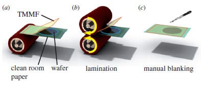
Figure 1. Lamination of the TMMF dry-film resist. (a) TMMF protected by a PET film is attached to standard clean-room paper carrying the wafer. (b) This sandwich is laminated between two heatable rubber-coated rolls. (c) After lamination, the wafer is cut out manually with a standard scalpel.
The TMMF resist was laminated to the wafer using a modified dry-film laminator from DuPont (RistonTM HRL rubber roller). The roller temperature, lamination speed (roller rotation) and lamination pressure (distance between rollers) had been adjusted for optimum performance.
To determine the distance between the lamination rollers, a commercial test gauge (Helios Type 23004007) was used— zeroed at the closed position of the laminator. At this point, the rollers are pressed together with a pressure higher than plam = 2 bar.
After lamination, the laminated wafer was cut out manually using a standard scalpel.
The second protective PET film can be peeled off the TMMF either before or after i-line illumination (365 nm). We used themask alignerMA6fromKarl S¨uss for the experiments presented in this publication.
For crosslinking of the illuminated TMMF resist, the wafer was cured on a standard hotplate (P.E.B. = postexposure bake). The resist can be developed with solventbased developer such as ethyl acetate or diacetate alcohol followed by isopropanol rinsing and rinsing in de-ionized water (DI water). For the experiments presented in this paper, we used two development steps (t1 = 4 min, t2 = 4 min) in the SU-8 developer (dev 600, 2-methoxy-1-methylethyl acetate) from MicroChem Corp. followed by 5min isopropanol rinsing and brief rinsing with DI water.
Finally, the developed and spin-dried photoresist structure was hard-baked in an oven at 200 °C for 1 h.
To seal the fabricated TMMF channel structure, a second layer was laminated and patterned in analogy to the first one (see figure 2).
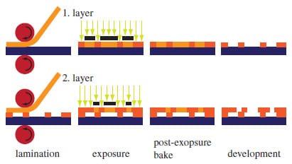
Figure 2. After the lamination of the TMMF dry-film resist, crosslinking is induced by patterned i-line (365 nm) illumination and finalized during the post-exposure bake (P.E.B.). After development in the solvent-based developer and hard-bake of the structure, further layers can be processed in a similar manner.
All relevant process parameters used for the fabrication of the first and second layers are listed in table 1.
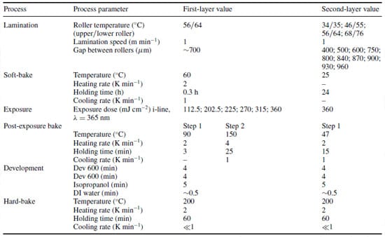
Table 1. Process parameters for the fabrication of structured channels in the TMMF dry-film resist on silicon wafers.
Due to its good chemical stability in acids, alkaline solutions and organic solvents [18], TMMF is suitable for diverse microfluidic applications. Nevertheless, in the case of reagent pre-storage, the long-term stability of the poly
mer (e.g. agent storage for drug delivery) has to be proven. Therefore, we incubated 55 µm thick TMMF test structures in several biologically relevant cleaning solutions, solvents and buffers for a period of 160 days (table 2). After incubation, the swelling behaviour of the TMMF dry-film resist was investigated by measuring the resist thickness using the surface profiler P-11 (Tencor).
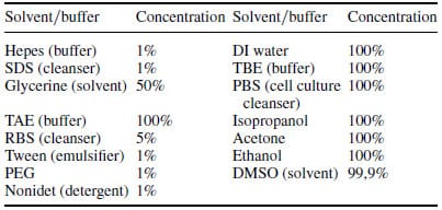
Table 2. List of biologically and microfluidically relevant solvents which were used for the long-term incubation (t = 160 days) of TMMF.
Furthermore, the cytotoxicity of the TMMFdry-film resist was tested according to the protocol of ISO 10993-5 for implantable medical devices.
For this purpose, a sterilized test material substrate was incubated for 24 h in the DMEM cell culture medium6 at a temperature of T = 37 °C with a specified ratio of the surface area to the cell culture medium of 6 cm² ml-1. A volume of V = 500 µl of the extract of this incubation was used to cultivate L-929 cells [40]. Approximately 150 000 cells were placed for this purpose into the wells of a 24-well plate 24 h before the experiment started and the cells were cultivated under standard conditions. After 24 h of incubation within the extract, the viability of the cells was tested by performing the Cell TiterGlo viability test7.
3. Results and discussion
3.1. First-layer fabrication
As the reliability and reproducibility of microfluidic structures strongly depend on adhesion, channel geometry and surface quality of the structure, the focus was initially set on the fabrication of the first layer. Due to different thermal expansion coefficients of TMMFand silicon (65 × 10-6 K-1 versus 3 × 10⁻⁶ K-1), fast and large changes in temperature have to be avoided during fabrication to avoid delamination effects, in particular, if large structure sizes are desired.
Therefore, for all temperature-dependent process steps, slow heating and cooling rates (ΔTmax = 2 K min-1) are applied. It was identified experimentally that a lamination temperature of Tupper roller = 56 °C/Tlower roller = 64 °C, a lamination speed of v = 1 m min-1 and a roller gap of droller = 700 µm assure homogeneous adhesion between the TMMF and silicon wafers or Si3N4 passivated silicon or Pyrex wafers, even for substrates with 600nmhigh topographies (e.g. metallization layers).
Figure 3 shows the difference in edge quality after illumination with and without the protective PET film.
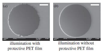
Figure 3. Effect of illumination through the protective PET film on the edge smoothness. The white scale bars represent 20 µm; (a) light is scattered and deflected by the PET film resulting in inhomogeneous side walls: I = 315 mJ cm-2 (b) excellent edge quality after illumination without the protective PET film: I = 202.5 mJ cm-2.
Due to the irregularities in surface smoothness of the structure side walls which resulted from illumination through the protective PET film (figure 3(a)), further illumination was performed after peeling the film off. The TMMFresist tends to stick to the glass/chromiummask during exposure without the protective PET film, but this can be prevented by performing a soft-bake at a temperature of Tsoft-bake = 60 °C for tsoft-bake = 20 min after removing the PET film.
Concerning the illumination during exposure, a clear dependence of channel width on the exposure dose can be observed, as illustrated by figures 4 and figure 5(a). Higher exposure doses lead to larger structure sizes and therefore to smaller channel dimensions due to overexposure and T-topping effects.
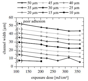
Figure 4. Influence of exposure dose on achievable channel width for different structure sizes of the lithography mask. Higher exposure doses result in smaller channels due to overexposure effects. Too low exposure results in poor adhesion as marked by parentheses.
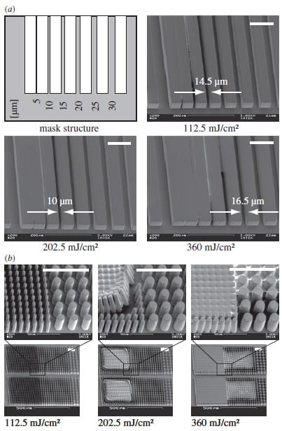
Figure 5. SEM images of TMMF test structures illuminated with different exposure doses. Whereas low exposure doses (I = 112.5 mJ cm-2 and I = 202.5 mJ cm-2) allow high aspect ratios of up to 7:1 for single free-standing structures, overexposure (and T-topping) effects limit aspect ratios (~ 3:1) for the highest exposure dose (I = 360 mJ cm-2). Additionally, waveguide effects due to changes in the refractive index during polymerization result in linked structures clearly visible in the pin structures on the left. The minimal channel width changes from w = 6 µm to w = 20 µm when the exposure dose is raised. Since partial delamination effects occur for exposure doses lower than I = 200 mJ cm-2, an exposure dose of I = 112.5 mJ cm-2 cannot be recommended. The white scale bars represent 100 µm.
For a resist thickness of dresist =45 µm, aminimal channel width of wchannel = 10 µm (aspect ratio: 9:2/height:width) has been achieved with an exposure dose of I = 202.5 mJ cm-2 (with 15 µm wide mask structures). It should be noted that lower exposure doses result in poor adhesion since only the top layer is illuminated (e.g. I = 112.5 mJ cm-2, ~10% delaminated structures).
As illustrated by the partially collapsed pin structures in figure 5(b), in addition to the structure enlargement, higher exposure doses or higher aspect ratios lead to additional illumination of small gaps due to optical waveguide effects that are caused by changes in the refractive index during illumination. For example, gelation of the resist due to the exposure, as described by Zhang et al [41], results in a visible change of the refractive index of the resist.
Therefore, the achievable aspect ratio for channel structures is smaller than that for free-standing structures. Free-standing structures have been fabricated with an aspect ratio of 7:1 (6.4 µm pins from 5 µm large mask structures).
3.2. Second-layer fabrication
The most challenging aspect of sealing shallow microfluidic cavities with extremely small height-to-width ratios is to achieve leakage-free seals without sagging of the lid structure.
Experiments have shown that the lamination pressure and lamination temperature have significant impact on the sealing quality.
If the lamination pressure is too low, adhesion fails and if the pressure is too high, sagging results. For the presented experiments, the adhesion pressure is determined by the distance between the two rollers (Shore Durometer Type A 60). As illustrated in figure 6, a relatively large process window (drollers min = 600 µm, drollers max = 900 µm) leads to good results for a combined thickness of the substrate of dsub = 660 µm (clean room paper + wafer + first TMMF layer). Within this process window, corresponding lamination pressures between plam, min = 0.9 and plam, max = 1.9 bar (measurement accuracy ± 0.2 bar) for drollers min = 750 and drollers max = 900 µm have been identified. To determine the lamination pressure, the applied pressure was measured by sealing a structured TMMF layer (~2/3 structure, ~1/3 gaps) with FujiFilm Prescale®</sup > pressure-sensitive film (4LW). The values were determined using FujiFilm’s computer-assisted read-out software.
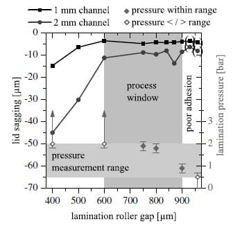
Figure 6. Influence of lamination pressure defined by the geometrical distance between the lamination rollers on the sagging of the lid structure spanning wide channels (w1 = 1 mm, w2 = 2 mm). A relatively large process window of Δdrollers = 300 µm allows good results for a thickness of d = 660 µm of the combined substrate, which is laminated together with a 45 µm thick TMMF layer. Within this process window, a lamination pressure of 0.9 bar < p < 1.9 bar leads to sag-free sealing of wide channel structures.
In addition, the sealing quality depends on the lamination temperature. While a low lamination temperature (e.g. Tupper roller = 34 °C/Tlower roller = 35 °C) results in delamination if the laminate is mechanically stressed, higher lamination temperatures increase creeping effects which lead to sagging of the lid structure (figure 7). For these experiments, the lamination temperature has been varied during lamination with a constant speed of v = 1 m min-1 and a roller distance of droller = 875 µm. Concerning adhesion and lid sagging, adequate results were achieved only with lamination temperatures of Tupper roller =46 °C/Tlower roller = 55 °C. Further experiments have shown that the lamination temperature has to be calibrated accurately with ΔT < 5 °C.
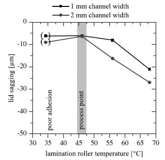
Figure 7. Influence of lamination temperature on the sagging of the lid structure spanning wide channels (w1 = 1 mm, w2 = 1 mm). Adequate results could only be achieved by using a lamination temperature of T = 46 °C. Only the temperature of the upper roller is shown in this figure; the corresponding temperature of the lower roller is defined in table 1.
It should be mentioned here that wetting issues also play a dominant role for the adhesion of the laminated layers. To omit irregularities, all wafers are dried on a hotplate for 1 min at 110 °C before lamination.
As the lamination temperature is raised, more and more short-chained polymer molecules of the uncured TMMF resist become liquefied. This effect was double-checked by performing a soft-bake of the laminatedTMMFresist on top of a structured TMMF layer (figure 8) under optical observation. Starting at room temperature, initial very slow creeping effects of the uncured resist can be monitored at a temperature of T = 40 °C.
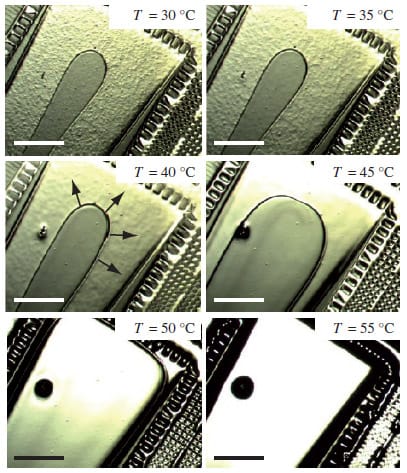
Figure 8. Optical investigation of the liquefaction of the uncured TMMF dry-film resist during a soft-bake. A second-layer TMMF is laminated onto a structured base substrate. At a temperature of T = 40 °C, first very slow creeping effects of the uncured resist can be observed. At T = 48 °C or higher, a considerable flowing of resist was monitored. These flowing effects immediately lead to lid sagging and channel clogging. The scale bars represent 1 mm.
For temperatures higher than or equal to T = 47 °C, considerable flowing of resist was observed. Here, a clear correlation to the reported glass transition temperature (Tg) of Tg = 49.5 °C [42] for non-crosslinked SU-8 is in evidence. Considering this creeping effect, a soft-bake at T = 60 °C as mentioned in section 3.1 cannot be performed after lamination on structured substrates. Further experiments have shown that for the drying of the resist surface to prevent sticking on the mask, the soft-bake temperature can be reduced to room temperature if the duration is extended to t = 24 h.
The influence of the lamination parameters is illustrated in figure 9. For channel widths of w < 500 µm, an adequate seal (adhesion between layers exceeds the mechanical stability of the lid structure) without or with only negligible sagging effects can be achieved with a calibrated lamination temperature of T = 46 °C.
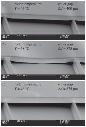
Figure 9. SEM images of partially sealed 500 µm wide channels with different lamination parameters. (a) High lamination pressures lead to squeezing of the resist in the contact areas. For wide channels (w > 700 µm), sagging also occurs. (b) High lamination temperatures lead to liquefaction of uncured TMMF resulting in immense sagging and squeezing of the resist. (c) By applying the right lamination parameters, perfectly flat spanning of channel structures can be achieved.
Another significant parameter is the duration of the illumination. While continuous illumination resulted in slight lid sagging (increase of sagging d ~ 10 µm for w = 1 mm wide channel) due to the rise in temperature, the best results were achieved by using discrete illumination cycles (I = 4.5 mJ cm-2 s; λ = 365 nm, i-line) of 5 s illumination with 10 s breaks which allowed the substrate to cool down between the illumination pulses.
Additionally, a similar creeping effect of the illuminated TMMF resist can be monitored during the post-exposure bake. Although crosslinking of the illuminated TMMF decelerates creeping effects, P.E.B. temperatures higher than T = 47 °C result in sagging of lid structures which span wide channels (> 500 µm), and liquefied TMMF can flow into the channel structures. This liquefaction effect caused problems particularly for tapered channels. Due to capillary forces, narrow or tapering channels are filled in advance and polymerization occurs there. Consequently, small channels become clogged.
By restricting the P.E.B. temperature to TP.E.B. = 47 °C (tP.E.B. = 15 min), the resulting creeping effects can be neglected for channel widths up to w = 2 mm (height h = 45 µm).
However, for lid structures illuminated with exposure doses lower than I = 300 mJ cm-2, streaking was observed (greasy surface and milky discolouration of the isopropanol) during the development step after the reduced P.E.B at TP.E.B. = 47 °C for tP.E.B. = 15 min. This streaking is caused by uncured parts of the resist.
To ensure complete curing of the illuminated photoresist, either the illumination dose has to be increased (I > 300 mJ cm-2) or the P.E.B. duration has to be extended (tP.E.B. < 30 min). However, increasing the illumination dose results in loss of resolution (minimal channel width wmin = 20 µm) and for extended P.E.B. durations (tP.E.B. > 30 min), the maximum sealable channel width is reduced to w ~ 1 mm.
Typically, the requirements on resolution of the lid structures (fluidic connections or vias) are lower than those for channel configurations. Therefore, we used an illumination dose of I = 360 mJ cm-2 and a reduced P.E.B. (TP.E.B. = 47 °C for tP.E.B. = 15 min) for the experiments presented in this publication.
Utilizing the laminated TMMF dry-film photoresist, wide and shallow cavities of a height-to-width ratio of 1:44 (45 µm:2 mm) were spanned (figure 10). Thereby, the adhesion of the two polymer layers exceeds the strength of the resist itself. At increasing stress, breaking of the substrate was observed before any delamination occurred. In contrast to all other experiments, the hard-bake step of the first layer was omitted in the experiment of figure 10. The consequence is an appa
rently rough surface on top of the layer structure which is presumably caused by residual solvents in the first layer that change the surface texture of the second layer. The mean roughness coefficients are Ra = 90 nm and Ra = 140 nm above the layer structure and cavity, respectively (Tencor P-11).
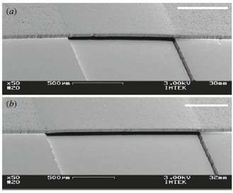
Figure 10. SEM images of partially sealed channels with large channel widths. (a) w = 1 mm, d = 45 µm. (b) w = 2 mm, d = 45 µm. The white scale bars represent 500 µm.
Concerning the applicability of agent pre-storage within microfluidic structures fabricated in the TMMFdry-film resist, we determined a small agent up-take (thickness variation Δd < 5%) of the TMMF test structures for all tested agents over the period of 160 days of incubation (figure 11). Nevertheless, it should be mentioned that the incubation in ethanol, acetone and DMSO resulted in occasional cracks on the surface of the resist which were clearly visible under the microscope.
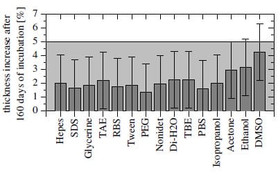
Figure 11. Swelling behaviour of the 55 µm thick TMMF dry-film resist during long-term incubation in biologically relevant solvents and buffers. After 160 days of incubation in acetone, ethanol and DMSO, the structures showed occasional cracks on the surface. For all other solutions, no extensive destruction effects occurred. The error bars have been determined from five measurements and represent the 3s confidence interval. For the reference layer of 55 µm, the confidence interval corresponds to ± 1.1 µm.
However, the TMMF dry-film resist did not show any destruction effects due to incubation in buffer solutions or solvents commonly used in cell cultivation and cell treatment.
Furthermore, the TMMF dry-film resist did not show cytotoxicity for the tested L-929 cell line according to ISO 10993-5 for implantable devices.
In contrast to the toxic positive control (tin-doped PVC slides) where the cells showed a viability rate of 0.44%, TMMF on silicon, silicon and a non-toxic negative control (Nunc Thermanox cover slides) did not affect the growth of the cells, represented by viability rates of 96.5%, 110% and 94.9%, respectively. All the mentioned viability rates have been standardized to a cell assay with pure fresh DMEM cell culture medium.
4. Conclusions
The applicability of the commercially available, epoxy-based, dry-film photoresist TMMF for the fabrication of microfluidic structureswas demonstrated and investigated in detail. TMMF was proven to be chemically stable and enables an aspect ratio of 7:1 for free-standing structures as well as 9:2 for channel structures. It can be laminated and processed on structured substrates with high topographies and enables the fabrication of sealed microfluidic structures. Extensive adaptation of prebaking steps, as is necessary e.g. to prepare SU-8 films suitable for lamination, can be omitted since the characteristics of the resist such as mechanical properties or solvent levels are already optimized by the producer of the dry-film resist.
Most challenging is the fluidic sealing of wide channel structures (up to w = 2 mm@d = 45 µm) without sagging of the lid structure. The sagging behaviour of the lid structures depends on lamination pressure and strongly on lamination temperature during lamination of the resist. Furthermore, the sagging is exacerbated by creeping of uncured resist parts whenever thermal energy is applied (soft-bake, illumination, or P.E.B.). To avoid adhesion between the resist and the lithography mask, the soft-bake can be replaced by storing the resist for t = 24 h at room temperature. The thermal energy transfer during illumination can be minimized by using multiexposure illumination. A reduced P.E.B. with temperatures below the glass transition temperature of the non-crosslinked resist (TP.E.B. = 47 °C for tP.E.B. = 15 min) allows channel structures with w = 2 mm to be spanned by the resist of thickness d = 45 µm with low lid sagging (<10 µm).
When compared to the spin-coating processing of SU-8, TMMR or comparable resists, the lamination of dry-film resists features the following advantages: (i) dry-film resists can be laminated onto structured substrates, (ii) dry-film resists feature very good thickness homogeneity (±0.6 µm for TMMF), (iii) the area which can be processed is not restricted by edge-bead removal steps and (iv) the processing speed is much higher than for spin-coating processes. Dry-film resists could revolutionize the fabrication of MEMS technology by marking a further step from two-dimensional processing to three-dimensional structures.
Acknowledgments
We gratefully thank the German Research Foundation (DFG, ZE 527/4) for financial support of this project. We also appreciate the good cooperation with the Cleanroom Service Center at IMTEK.
References
- Manz A, Graber N and Widmer H M 1990 Miniaturized total chemical analysis systems: a novel concept for chemical sensing Sensors Actuators B 1 244–8
- Ducr´ee J and Zengerle R 2004 Flow-Map—Microfluidic Roadmap for the Life Sciences, Books on Demand GmbH (Nordstedt, Germany: Books on Demand GmbH)
- Haeberle S and Zenglere R 2007 Microfluidic platforms for lab-on-a-chip applications Lab Chip 7 1094–10
- Thorsen T, Maerkl S and Quake S 2002 Microfluidic large-scale integration Science 298 580–4
- Solf C, Janssen A, Mohr J, Ruzzu A and Wallrabe U 2004 Incorporating design rules into the LIGA technology applied to a Fourier transformation spectrometer Microsyst. Technol. 10 706–10
- [6] Bertsch A, Jiguet S and Renaud P 2004 Microfabrication of ceramic components by microstereolithography J. Micromech. Microeng. 14 197–203
- Clerc P-A et al 1998 Advanced deep reactive ion etching: a versatile tool for microelectromechanical systems J. Micromech. Microeng. 8 272–8
- Bower D W, Ismail M S and Roberts B E 1993 Low temperature Si3N4 direct bonding Appl. Phys. Lett. 62 3485
- Steigert J et al 2008 Rapid prototyping of microfluidic chips in COC J. Micromech. Microeng. 17 333–41
- Xia Y and Whitesides G M 1998 Soft lithography Annu. Rev. Mater. Sci. 28 153–84
- Lin C-H, Lee G-B, Chang B-W and Chang G-L 2002 A new fabrication process for ultra thick microfluidic microstructures utilizing SU-8 photoresist J. Micromech. Microeng. 12 590–7
- Lorenz H, Despont M, Fahrni N, Brugger J, Vettiger P and Renaud P 1998 High-aspect-ratio, ultrathick, negative-tone near-UV photoresist and its applications for MEMS Sensors Actuators A 64 33–9
- Misumi K, Saito K, Yamanouchi A, Senzaki T and Honma H 2006 Minute tunnel structure formation with permanent film photoresist J. Photopolym. Sci. Technol. 19 57–62
- Mata A, Fleischman A J and Roy S 2006 Fabrication of multi-layer SU-8 microstructures J. Micromech. Microeng. 16 276–84
- NANO SU-8 2000 Negative Tone Photoresist Formulations 2002–2025 (Newton, MA: MicroChem Corporation)
- NANO SU-8 2000 Negative Tone Photoresist Formulations 2035-2100 (Newton, MA: MicroChem Corporation)
- Sato H, Matsumura H, Keino S and Shoij S 2006 An all SU-8 microfluidic chip with built-in 3D fine microstructures J. Micromech. Microeng. 16 2318–22
- St¨ohr U, Vulto P, Hoppe P, Urban G and Reinecke H 2008 High-resolution permanent photoresist laminate for microsystem applications J. Micro/Nanolith. MEMS MOEMS 7 033009
- Vora K D, Shew B Y, Harvey E C, Hayes J P and Pee
le A G 2005 Specification of mechanical support structures to prevent SU-8 stiction in high aspect ratio structures J. Micromech. Microeng. 15 978–83 - Han M, Lee W, Lee S-K and Lee S S 2004 3D microfabrication with inclined/rotated UV lithography Sensors Actuators A 111 14–20
- Bertsch A, Lorenz H and Renaud P 1999 3D microfabrication by combining microstereolithography and thick resist UV lithography Sensors Actuators A 73 14–23
- Gracias A, Xu B and Castracane J 2005 Proc. 9th µTAS Conf. (Boston) (Transducers Research Foundation, San Diego, CA, USA) vol 1 pp 663–5
- Tay F E H, van Kan J A, Watt F and Choong W O 2001 A novel micro-machining method for the fabrication of thick-film SU-8 embedded micro-channels J. Micromech. Microeng. 11 27–32
- Song I and Ajmera P K 2003 Use of photoresist sacrificial layer SU-8 electroplating mould in MEMS fabrication J. Micromech. Microeng. 13 816–21
- Liu G, Tian Y and Zhang X 2003 Fabrication of microchannels in negative resist Microsyst. Technol. 9 461–4
- Metz S, Jiguet S, Bertsch A and Renaud P 2004 Polyimide and SU-8 microfluidic devices manufactured by heat-depolymerizable sacrificial material technique Lab Chip 4 114–20
- Con´ed´era V, Salvagnac L, Fabre N and Zamkotsian F 2007 Surface micromachining technology with two SU-8 or SiO2/sol–gel sacrificial layers J. Micromech. Microeng. 17 N52–7
- Psoma S D and Jenkins D W K 2005 Comparative assessment of different sacrificial materials for releasing SU-8 structures Rev. Adv. Mater. Sci. 10 149–55
- Hu M, Lindemann T, G¨ottsche T, Kohnle J, Zengerle R and Koltay P 2007 Discrete chemical release from a microfluidic chip J. Microelectromech. Syst. 16 786–94
- Carlier J, Arscott S, Thony V, Fourrier J C, Caron F, Camart J D, Druon C and Tabourier P 2004 Integrated microfluidics based on multi-layered SU-8 for mass spectronomy analysis J. Micromech. Microeng. 14 619–24
- Tuomikoski S and Franssila S 2005 Free-standing SU-8 microfluidic chips by adhesive bonding and release etching Sensors Actuators A 120 408–15
- Jackman R J, Floyd T M, Ghodssi R, Schmidt M A and Jensen K F 2001 Microfluidic systems with on-line UV detection fabricated in photodefinable epoxy J. Micromech. Microeng. 11 263–9
- Bilenberg B, Nielsen T, Clausen B and Kristensen A 2004 PMMA to SU-8 bonding for polymer based lab-on-a-chip systems with integrated optics J. Micromech. Microeng. 14 814–8
- Blanco F J, Agirregabiria M, Garcia J, Berganzo J, Tijero M, Arroyo M T, Ruano J M, Aramburu I and Mayora K 2004 Novel three-dimensional embedded SU-8 microchannels fabricated using a low temperature full wafer adhesive bonding J. Micromech. Microeng. 14 1047–56
- Li S, Feidhoff C B, Young R M and Ghodssi R 2003 Fabrication of micronozzles using low-temperature wafer-level bonding with SU-8 J. Micromech. Microeng. 13 732–8
- Pan C-T, Yang H, Shen S-C, Chou M-C and Chou H-P 2002 A low-temperature wafer bonding technique using patternable materials J. Micromech. Microeng. 12 611–5
- Agirregabiria M, Blanco F J, Berganzo J, Arroyo M T, Fullaondo A, Mayora K and Ruano-L´opez J M 2005 Fabrication of SU-8 multilayer microstructures based on successive CMOS compatible adhesive bonding and releasing steps Lab Chip 5 545–52
- Steigert J, Brett O, M¨uller C, Strasser M, Wangler N, Reinecke H, Daub M and Zengerle R 2008 A versatile and flexible low-temperature full-wafer bonding process of monolithic 3D microfluidic structures in SU-8 J. Micromech. Microeng. 18 095013
- Abgrall P, Lattes C, Con´ed´era V, Dollat X, Colin S and Gu´e1 A M 2006 A novel fabrication method of flexible and monolithic 3D microfluidic structures using lamination of SU-8 films J. Micromech. Microeng. 16 113–21
- Drexler H G, Dirks W, MacLeod R A F, Quentmeier H, Steube K G and Uphoff C C 2001 DSMZ Catalogue of Human and Animal Cell Lines 8th edn (DSMZ: Braunschweig)
- Zhang J, Chan-Park M B and Connor S R 2004 Effect of exposure dose on the replication fidelity and profile of very high aspect ratio microchannels in SU-8 Lab Chip 4 646–53
- Feng R and Farris R J 2003 Influence of processing conditions on the thermal and mechanical properties of SU-8 negative photoresist coatings J. Micromech. Microeng. 13 80–8


