


Semiconductor production

Verifying CMP head contact uniformity

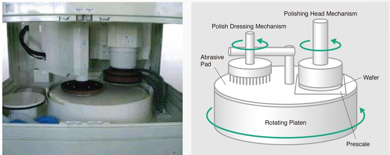
CMP* is a process for polishing the surface of silicon wafers. It involves mounting a silicon wafer parallel to an abrasive pad, rotating the wafer and pushing it against the abrasive pad along with a polishing slurry. High precision is necessary as the amount of polishing required is extremely small.
Presviously, the contact uniformity of the silicon wafers and the abrasive pads had generally been controlled by examining the polishing results. Production would sometimes continue despite unresolved instances of poor polishing, and there were other issues including inadequate contact precision that frequently resulted in low quality
Presviously, the contact uniformity of the silicon wafers and the abrasive pads had generally been controlled by examining the polishing results. Production would sometimes continue despite unresolved instances of poor polishing, and there were other issues including inadequate contact precision that frequently resulted in low quality
*CMP: Chemical Mechanical Polishing

Prodcut used: Prescale (Extremely low pressure 4LW)
Prescale is placed on the abrasive pad, after which the silicon wafer is set in the polishing head and pressure is applied. The pressure is then released, the Prescale removed and resulting color of the Prescale is examined whether pressure had been uniformly applied.

[Not good]
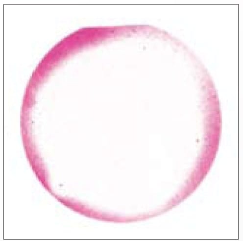
Pressure is uneven
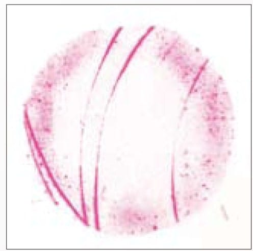
Abrasive pad is scratched.
[Good]
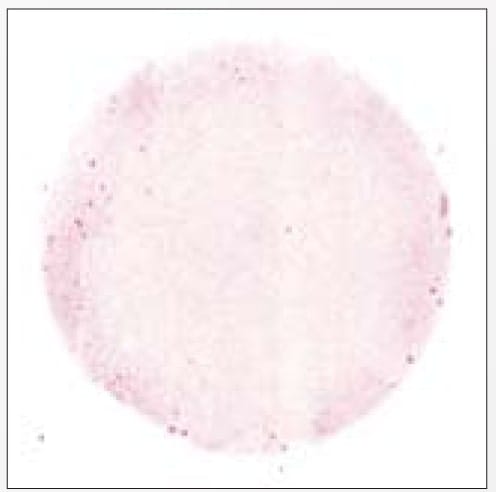

Time savings
Contact uniformity can be adjusted during the design stage, resulting in greatly improved design efficiency.
Quality improvement
Contact uniformity can be preiodically checked during maintenance, and at other times, thus facilitating stable production quality. Additionally, the variance between CMP units can be controlled.
Without using Prescale
When productionn problems can only be inferred from the polishing results, trial and error adjustments are required. Silicon wafer material losses occur and additional time is required for servicing etc.

Using Prescale
Prescale makes it possible to verify the pressure applied to the silicon wafer under actual use conditions. Time reduction and improved quality can be achieved because knowledge applicable to polishing uniformity and polishing speed adjustments can be obtained.


