Article: MST News
Th. Schreier-Alt T. Braun, K.-F. Becker, Ch. Rebholz, B. Wunderle and H. Reichl
Introduction
To keep Printed Circuit Boards (PCBs) the standard platform for most electronic products, great efforts have been made to create an innovative, multi-functional board with increased technological value. A central aspect of this “innovative PCB” is to bridge the gap from the steadily miniaturizing ICs to our “outside world” of macroscopic dimensions. This ever-lasting question of packaging – how to keep up with Moore’s Law – is now being enlarged by the designs of “More than Moore” [1]. Two established technologies can be a key towards creating the “innovative PCB”: 1. Flip chips are widely used to achieve highest miniaturization within microelectronics packaging. 2. Transfer moulding with epoxy moulding compound (EMC) has been the standard process for reliable single chip encapsulation for decades. The combination of both technologies is one method of choice for packaging miniaturization and has proven to be a highly reliable encapsulation technique, also on FR-4 substrates [2, 3].
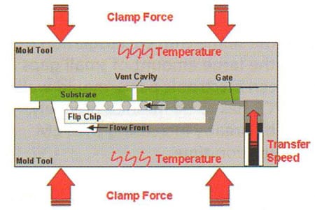
Figure 1: layout of a single flip chip on PCB encapsulation process: the same polymer is used for underfiller and glob top.
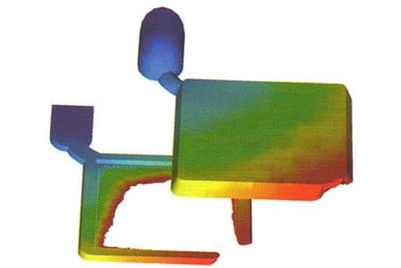
Figure 2: Simulation of Flip Chip Encapsulation process: flow front after filling of glob top space.
Especially the simultaneous underfilling and overmoulding of flip chips by transfer moulding can greatly enhance bump reliability as the low coefficient of thermal expansion (CTE) of the molding compound reduces thermal mismatch.
Full advantages are achieved by combining moulded underfill and batch processes on substrate level. Moulded Area Package (MAP) geometries enable flexible production of complex mUlti-chip modules. Trends of the market clearly drive towards these high-density Systems in Package (SIPs), where classical underfilling is limited. If based on standard FR-4 substrates, this technology additionally enables high productivity and optimized costs. Flip Chip Encapsulation on PCB The process of flip chip encapsulation on PCB is shown in fig. 1. The epoxy is injected at the gate, simultaneously covering and underfilling the chip.
To red.uce production related stress, the encapsulation process was analyzed by finite element simulation (FEM). CFD simulations often overestimate the filling ability within small gaps. They ignore the enlarged flow resistance caused by high EMC filler content. For flip chip encapsulation, particle diameters are <25μm, but nevertheless should not be neglected. The estimated filling behaviour shows a highly unbalanced flow due to the different gap sizes (fig . 2): when the 300 μm cavity on top of the chip is filled completely while the 80 μm underfiller gap is only filled at its edge parts.
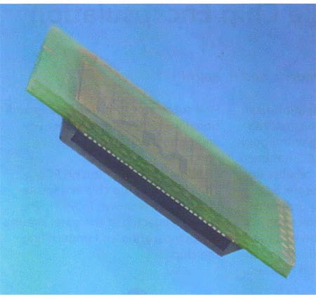
Figure 3: Flip Chip on PCB.
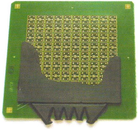
Figure 4: MAP moulding on FR-4 board without electronic parts.
This unbalanced flow can cause an abrupt pressure increase at the moment the mould cap is filled, but the underfilling still commences. The pressure acts mainly on the top side of the chip and can deform solder bumps and even crack chips [2]. By transferring pressure and temperature values from CFD simulation to a structural simulation tool, the viscoelastic response of the solder can be calculated . Consequently, the process simulation can propose optimized machine and CAD parameters.
Reliability of chips underfilled by Transfer Moulding
Moulded flip chips show a much higher reliability than packages with capillary underfill. All moulded devices passed Moisture Sensitivity Test Jedec Level 1 and more than 3000 h at 85°C / 85% relative humidity without any electrical failures or delaminations. Temperature cycling from 55°C up to 125°C revealed an extremely high reliability. Moulded Flip Chips passed more than 14.000 cycles without electrical failures. This is more than five times higher than standard flip chips assemblies on FR4 may withstand .
The experimental reliability investi gations were backed by thermo-mechanical FEM simulations. As failure criterion, the inelastic accumulated creep strain in the solder bumps was : used within a Coffin-Manson approach.
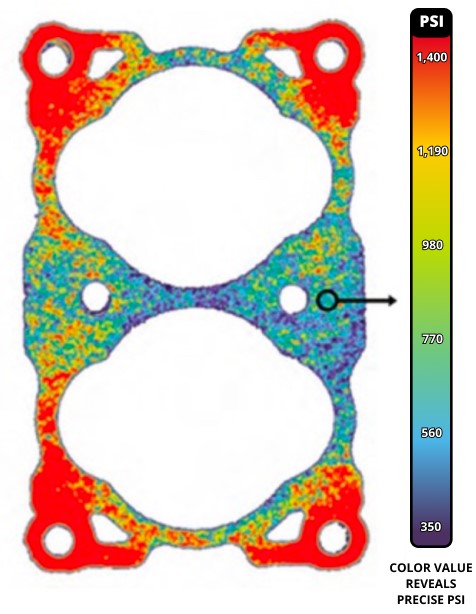
Figure 5: Pressure distribution during MAP moulding.
Left: predicted by numerical simulation, right: pressure-indicating film.
Simulations can explain the extreme lifetime of the flip chip assemblies based on the favourable stress distri bution generated by the encapsulation: First, the local thermal mismatch is quite low, as the CTE of the solder equals nearly the CTE of the gap materials: The CTE of the moulding compound is unusually low in or der to compensate the corresponding high value of the solder mask. Secondly, the PCB is thin (0.8 mm), which is known to be an important factor for flip chip reliability [4]. The third aspect could be due to the EMC itself: It reduces the bending of the chip and at the same time compresses the die. Due to a stress redistribution the local stresses in the bump are shifted towards the interface between encapsulant and die. So moulding of a flip chip can greatly enhance bump reliability if at the same time a perfect adhesion of EMC can be assured.
Map Moulding on PCB
The advantages of moulded underfill processes pushed their adaptation to MAP-type geometries for Systems in Package (SiP) modules. Nevertheless the flow behaviour of a moulding compound on multi-chip substrates, containing a heterogeneous variety of devices, is far more complicated than the single chip encapsulation. First, the large amount of small gaps between electronic parts, mould wall and PCB has to be meshed precisely, thereby greatly increasing the FEM computation time.
Secondly, the additional flow resistance of EMC filler particles has to be taken into account.
Thirdly, the flow front can get very complicated during overmoulding of large substrates, even if no electronic components at all are present. An example is shown in fig . 4: the short shot shows a tendency for inhomogeneous filling due to thermal warpage of the substrate. Different metallization densities on top and bottom PCB side can cause a (here: convex) bending of the board after exposure to the hot mould tool. This causes an increased material flow on both panel sides and might lead to air traps and unfilled modules. In the present case, the warpage disappears after assembling components with a lower CTE compared to FR-4.
Homogenous material flow and pressure distribution within the cavity is of particular importance for encapsulation of mechanically sensitive parts, e.g. MEMS. With the use of pressure sensitive films a fast and inexpensive estimation of the pressure distribution can be achieved. Our multilayer film design is based on commercially available colour changing papers (e .g. Prescale™ ), an adhesive layer and an isolating pqlyimide film. This enables tests for several minutes at 180°C without detraction of the sensor function . Their accuracy is ~10%, checked by conventional pressure sensors located at different positions within the mould walls. The pressure results also fit well with numerical simulations (fig. 5).
Conclusions
Flip chip encapsulation with simultaneous underfilling and overmoulding has proven to be a highly reliable encapsulation technique on high Tg FR- 4 substrates. The combination with MAP-type overmoulding enables cost-attractive production of various multi-chip module layouts. Together with integrated optical functions and embedded components, the printed circuit board technology will stay an innovative, attractive and nevertheless coefficient electronic platform.
Acknowledgements
Parts of this work have been funded by the Mikrosystemtechnik Bayernprogramme.
References
- H. Reichl, K.-D. Lang; Heterogeneous Integration for Smart Systems; EURIPIDES Forum, Berlin, October 9-1 Oth, 2008
- Y. K. Shen, T. W. Ye, S. L. Chen, C. H. Yin, W. D. Song; Study on Mold Flow Analysis of Flip Chip Package. Int. Comm. Heat Mass Transfer, Vol. 28, No.7, pp. 943-952, 2001
- T. Braun et al.; Improved Reliability of Leadfree Flip Chip Assemblies Using Direct Underfilling by Transfer Molding. International Electron ic Manufacturing Technology Conference IEMT, Putrajaya, mst I news 2 09 Malaysia, 2006.
- B. Wunderle, W. Nüchter, A. Schubert, B. Michel, H. Reichl. Parametric FE-approach to flip-chip reliability under various loading conditions. Journal of Microelectronics Reliability, 1933-1945,2004.
Authors:
Thomas Schreier-Alt,
Tanja Braun,
Karl-Friedrich Becker, Christian Rebholz,
Bernhard Wunderle,
Herbert Reichl
Fraunhofer Institute for Reliabilityand Microintegration, Berlin and Oberpfaffenhofen, Germany


