Article: Electronic Products
For heat sinks to work most efficiently, users must see that they are designed and installed so as to maximize heat flow
Modern microprocessor-controlled electronics and high-power LED-based lighting operate at elevated temperatures due to Joule heating. As a result, the use of heat sinks to dissipate temperature has become very important in electronic system designs. But for heat sinks to work most efficiently, users must be certain that they are installed in such a way as to maximize heat flow. This can only been done if engineers make the correct measurements using appropriate sensors when installing heat sinks.
Basic heat sink operation
Heat conducted from the electronic component to the heat sink is governed by Fourier�s law of heat conduction:
q = -k x A x dT/dx
where q is the heat conducted, k is the thermal conductiv- ity of the heat sink, A is the cross-sectional area through which heat is conducted, and dT/dx is the temperature gradient between the heat sink and the component being cooled. So it follows that the amount of heat conducted into the heat sink is directly proportional to the cross-sec- tional area, �A,� through which that heat is conducted.
When there is uneven contact between the heat sink and the electronic component, the value of �A� is re- duced, as is the resulting amount of heat conducted. Such uneven contact manifests itself in variations in the pres- sure distribution between the two adjacent surfaces.Therefore, it is important to measure the pressure profile on mating surfaces to assure optimum contact.
Fig. 1. Pressure-indicating film is used to properly mount the heat sinks in for ABB�s Press-pack High Power Semiconductor (left). Uniform pressure distribution between the heat sink and the semiconductor is seen in the film at top, where the white area is a hole in center of the film for a heat-sink mounting screw. In contrast, when there is poor pressure distribution (bottom), the film shows deep red areas of high pressure and white areas where there is very little contact between the heat sink and the semiconductor.
Unfortunately, many manufactur- ers do not attempt to quantify the pres- sure profile. They rely instead upon tightening mounting screws using uni- form force, which they assume will lead to even pressure distribution. But tightening the screws without some method to reveal pressure distribution at the surface can cause warpage or dis- tortion of the heat sink or of the elec- tronic component. This, in turn, can lead to loss of contact or uneven pres- sure distribution between the mating surfaces.
Pressure-sensing approaches
Traditionally load cells have been used to measure pressure. However, they only measure the overall force exerted upon the two surfaces, not the pressure distribution across the entire surface. They provide no in- formation on the pressure gradients between the surfaces. The omission of this vital pressure distribution data can have serious consequences.
The need to measure pressure dis- tribution at the surface has led to the development of two specialized meth- ods. The first involves the use of pres- sure-indicating sensor film. The sec- ond method involves the employment of electronic tactile surface-pressure mapping systems, which reveal how pressure is exerted between two sur- faces in real time.
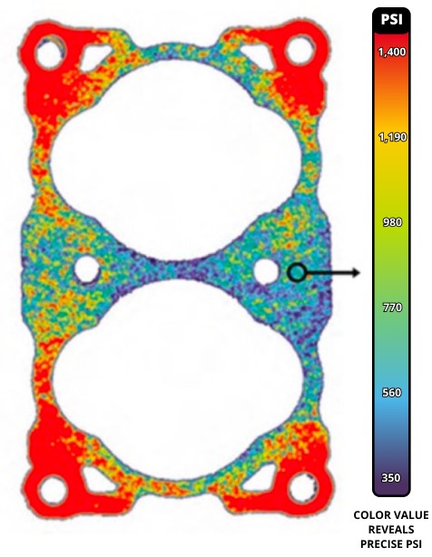
Researchers have used tactile pres- sure-indicating sensor film for the past 20 years to study heat conduction and have reported the results in heat sink literature. Pressurex® sensor film is a thin Mylar-based film that contains a layer of tiny microcapsules that burst upon the application of force to pro- duce an instantaneous and permanent high- resolution image of pressure vari- ation across the contact area. This film can be placed between two surfaces that touch, mate, or impact. When the film is removed, the pressure distribu- tion profile � which shows where variations in pressure occur between contacting surfaces � is immediately visible on the film.
Conceptually similar to Litmus pa per, the change in color intensity of the film is directly proportional to the amount of pressure applied to it � the greater the pressure, the deeper the color. The color variations in the film can reveal surface pressures from 2 to 43,200 psi (0.14 to 3,000 kg/cm2).
Practical examples
ABB Switzerland Ltd recommends the use of pressure-indicating film during the setup and mounting of their wa- ter-cooled Press-pack High Power Semiconductors heat sinks (fig. 1). The film is used to prevent uneven pressure that will lead to deformation of the housing and internal stress be- tween the different device layers, causing it to fail prematurely during load cycling.
Many manufacturers routinely use pressure-indicating sensor film (man- ufactured by Sensor Products under the Pressurex® brand) to diagnose pres- sure distribution in their designs. For example, Robin McCarty of Marlow ndustries uses the film to investigate thermal interfaces between thermo- electric power generators and heat sinks and identify the high spots.
Marc-Jason Renaud of Curtis-Wright Corp. uses sensor film to evaluate the compressive force ap- plied on circuit-card-assembly com- ponents when their thermal frames are installed. The forces on the com- ponents must be minimized to pre- vent long-term operational damage.
Tactile pressure-indicating sensor film is also used in other electronics- related processes, including wafer bonding and polishing, printed circuit board and other lamination press ap- plications, and LCD panel displays.
Surface-pressure mapping
Electronic surface-pressure mapping allows the engineer to measure actu- al, real-time contact force and pres- sure distribution data. This technique provides time-dependent pressure in- formation, unlike pressure-indicating ilm, which provides a static �snap- shot� of a maximum pressure profile.
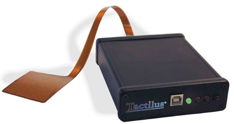
Using systems such as the Tactilus® developed by Sensor Products Inc., de- sign engineers can confirm FEA pre- dictions as well as monitor the chang- ing surface pressure between components during assembly. Since the sensors are thin and flexible, they can be placed between two contacting surfaces with minimal affect on the overall assembly. This matrix-based technology utilizes resistive sensors where the resistance of the sensing point is proportional to pressure.
Electronic surface-pressure map- ping is especially useful in develop- ing procedures for mounting heat sinks. Both chipset and heat sink surfaces are rigid, and can have as few as three points of contact be- tween them. This could lead to very high localized pressure dur- ing the assembly process. Tactile pressure mapping allows the en- gineer to monitor the pressure distribution while the assembly is torqued to minimize the stress on the chip and to assure that the final mounting parameters result in even pressure distribution between all components.
 |  |  |
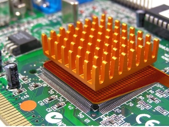
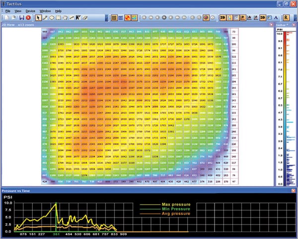
| Fig. 2. With the Tactilus® Sensor system (left), a 25 x 25 array of sensors can be placed between a CPU and a copper heat sink (center, note that the sesor is specifically sized to the chip). The data collected in this way is used to generate pressure maps (right; green represents low pressure, orange higher pressure), graphs, and statistics | ||
The Tactilus® surface-pressure mapping system specifically mea- sures the interface between proces- sors and their heat sinks (see Fig. 2). The sensing element is 50 x 50 x 0.38-mm thick, has 625 total sens- ing points in a 25 x 25 array, and a pressure-sensing range of 0 to 100 psi (0 to 7 kg/cm2). The element can be scanned at a rate of 100 times/s and data from the sensor points are collected and processed using a pro- prietary Windows-based tool kit. The technology also uses advanced elec- tronic shielding techniques to maxi- mize the sensor�s immunity to noise, temperature, and humidity.
A leading large-computer manufac- turer in the U.S. is using this technol- ogy, and it has also been used to aid in the selection of thermal material used in conjunction with heat sinks.
In one instance, the thermal mate- rial required 125 psi for it to align in a direction where it would conduct heat. When the parts were assembled, Tactilus® found that the heat sink warped from the force of the mount- ing bolts. As the heat sink distorted, it lost contact with the bottom plate, resulting in low contact pressure over 80% of the interface.
Sensor film in manufacturing
Heat sinks are used in many manufac- turing operations to transfer heat to and from parts being assembled. Josea Marias of Foxconn uses pressure-indi- cating sensor film for calibrating a heat/pressure bar in bonding machines that adhere Chip on Flex devices to liq- uid crystal display panels. The bar pres- sures and heats the assembly to achieve bonding. Macias said that the pressure- indicating film is very helpful in deter- mining which tilt adjustments to make to achieve the proper contact pattern between the bar and the assembly.
Pressure-indicating film is also use- ful in ensuring heat flow during weld- ing and joining operations. This is par- ticularly important for the power industry. As a general practice, new tooling should be checked for proper operation before being used in any manufacturing operation and, once in place, production tooling should also be routinely checked as part of a peri- odic maintenance regimen.


