Article
Related Links
Sung-Won Youn *, Akihisa Ueno, Masaharu Takahashi, Ryutaro Maeda
Advanced Manufacturing Research Institute (AMRI), National Institute of Advanced Industrial Science and Technology (AIST), 1-2-1 Namiki, Tsukuba, Ibaraki 305-8564, Japan
Abstract
In this study, we explored a rapid and low-cost process for patterning in a SU-8 photoresist by thermal imprinting with a non-transparent mold such as Ni mold. One of major obstacles in the process is that the extremely good formability of uncured SU-8 even near room temperature causes the collapse of imprinted patterns during and after de-molding because a sample cannot be exposed to UV light during imprinting owing to the non-transparency of a mold. To overcome this problem, un-cured SU-8 resists were pre-treated with UV light, heat, and O2 plasma for controlling their formability, and applied to thermal imprint tests to be compared each other in terms of the replication fidelity. As a result, a SU-8 sample pre-treated with UV light for 8 s resulted in the best replication quality for given imprint conditions and mold dimensions, and we could successfully replicate micro patterns in SU-8 resist without a quartz mold. As compared with conventional UV-imprint processes, this process has potential merits such as a lower mold cost, an easier mold release and a less air-entrapment.
1. Introduction
SU-8 is a kind of epoxy-based thermoset/UV-curable negative photoresist. Cured SU-8 has excellent chemical and thermal stability because of the highly cross-linked matrix in the exposed material, making it well suited for various permanent use MEMS devices [1,2].
Although SU-8 was originally developed for a micromachining process such as UV-photolithography [3], un-cured SU-8 has several attributes (e.g., low glass transition temperature of 60 °C and good formability) which make it suitable for imprint lithography such as an UV-imprint process. Recently, there have been several reports regarding the UV-imprint of SU-8 [4–6] because imprint lithography offers decisive technical potential to produce nano/micro structures with high throughput at a low cost. One of key advantages of UV Imprint lithography is that it can fabricate nano/microstructures on permanent use UV curable resist at room temperature under low pressure (<0.5 bar) [7–11]. A lower imprint temperature leads to a better layer-to-layer overlay accuracy, a less thermal residual stress, and a less degradation of mold surface coated with a mold release agent.
Nevertheless, there still remain other critical issues that need to be more studied for the expansion of applicable fields of UV-imprint technologies in industry. One of them is the relatively high cost for quartz mold fabrication. Conventional UV-imprint lithography of SU-8 resists requires the mold of optically transparent material, such as quartz, because the SU-8 sample has to be exposed to UV light during imprinting step. By UV radiation and heating above a critical temperature during an imprinting step, a strong acid (HSbF6) is generated, which causes the epoxy resin to form a ladder-like structure with a high cross-linking density. Main problem is that a quartz micro mold is technically more difficult to be prepared and much more expensive as compared to a conventional Si or Ni mold, particularly for that has positive patterns with complex vertical geometries (e.g., mold for micro scale dual-damascene structures) [12].
This study aimed to develop a process that forms micro pattern in SU-8 by thermal imprinting with a non-transparent mold such as a Ni mold. One of major concerns of the process is that un-cured SU-8 is too soft even at room temperature so that imprinted patterns deform during and after de-molding due to their time-dependent deformation behavior. To overcome this problem, we modified an imprint process, which involves a surface pre-treatment of un-cured SU-8 resist, followed by thermal imprinting (<90 °c). the major role of pre-treatment was formability control un-cured su-8. series thermal imprint tests were performed using su-8 samples with and without pre-treatments (uv light, heat, o2 plasma) and their results were compared each other in terms of the replication fidelity. Imprint test results were evaluated and compared with respect to the replication fidelity. Finally, we investigated the imprint conditions to replicate micro patterns in the SU-8 resist.
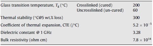
Table 1 – Thermal and electrical properties of SU-8
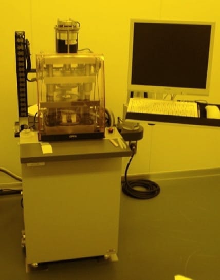
Fig. 1. Photograph of desk-top imprint equipment.
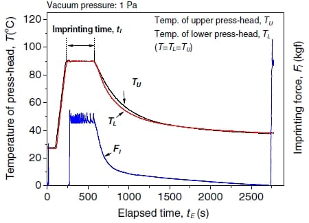
Fig. 2. Typical imprinting conditions history.
2. Experimental details
Commercially available SU-8 3000 (Microchem Corp., USA) was used as an imprint material. Vendor information regarding the thermal and electrical properties of SU-8 is listed in Table 1. The glass transition temperature of uncrosslinked SU-8 is 60 °C, making it suitable for a low-temperature imprint process. Thermal-imprint tests were performed in desk-top imprint equipment, which is designed to imprint 3 x 3 cm2 samples, as shown in Fig. 1. The available maximum heating temperature for press-punch is 700 °C, and the maximum press force is 200 kgf. A pumping system allows imprinting samples under a vacuum, with a pressure of 1 Pa inside the chamber. Prior to imprinting, local flatness distortions in the mold and/or sample were evaluated using a pressure-sensitive film (Prescale film, Fuji-Film Co., Japan), and compensated. Unless otherwise indicated, a GC-1720 (Sumitomo 3M, Japan) solution was used as a mold release agent. The thickness of SU-8 films was measured using a microfigure measuring instrument (Surfcorder ET4000M, Kosaka. Laboratory Ltd., Japan). The surface morphologies of Ni molds and imprinted surfaces were observed with a scanning electron microscope (SEM). The surface topographic properties of Ni molds and imprinted samples were measured with an interferometric surface profiler (Zygo New View 5000, Zygo Corp., USA) and a confocal scanning laser microscope (five-line confocal scanning laser microscope, OPTELICS S130, Lasertec Corp., JAPAN).
3. Process flow
SU-8 films with a thickness of about 50 lm were coated on Si wafers by spin-coater. To improve the adhesion of a SU-8 onto Si, 4-in. Si wafers were etched using a SF6 plasma for 2 min, and spin-coated with an HMDS before SU-8 coating. The SU-8 coated Si wafers were then cut into 15 x 15 mm2 by dicing. After spincoating of SU-8, all SU-8/Si samples were pre-
baked on a level hot plate at 95 °C for 30 min to evaporate the solvent and densify the film. Prior to imprinting, the surfaces of samples were then pre-treated by heating, UV-exposure, and O2 plasma to control the formability. The procedures of the imprint process adapted in this study were as follows. In the first step, a mold is pressed into the SU-8 resist at set temperature (well above Tg of un-cured SU-8; 60 &Deg;C) to physically deform the resist shape such that it conforms to the topology of the mold. Fig. 2 shows the typical process condition history used in this study. Imprinting temperature condition for un-cured SU-8 has been reported elsewhere and a rule thumb of is that imprint temperature should be set below 95 °C to prevent degassing. The temperature for upper punch (TU) and lower punch (TL) was set to the same value. The imprinting velocity and the heating rate were fixed at 50 lm min-1 and 0.5 °C s-1, respectively.
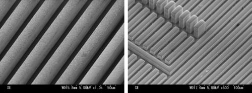
Fig. 3. SEM images of the micro patterns in the Ni molds; (a) pattern with 25 &um;m height and 10 &um;m width/spacing, (b) pattern with 10 &um;m (partially 30 &um;m) height and 10 &um;m width/spacing.
The imprinting temperature that is higher than pre-bake temperature can cause the de-gassing phenomena. To achieve uniform distribution of pressure over the entire sample surface, a polymer spacer was inserted between the SU-8 sample and the lower press-head surface. The pressing pressure then maintained for sufficient time to achieve complete filling. This hold time is the function of both material temperature and pressing force. After cooling to <40 °C in vacuum, the applied force was released and the Ni mold was removed from the SU-8 resist in the un-cured state. In the final step, the imprinted SU-8 resist is post cured with exposure to UV light and subsequent baking. De-molding process has to be carried out prior to post-bake procedure because the highly cross-linked SU-8 is extremely difficult to be removed.
4. Results and discussion
4.1. Ni mold fabrication
A positive Ni mold with the size of 20 x 20 mm2 for thermalimprinting was prepared by a Si micromachining process and a damascene process. The fabrication process of the Ni mold starts with a Si micromachining process, such as deep reactive ion etching (RIE) using the standard Bosch process. After sputtering seed and barrier metallic layers on the Si master, Ni was electroplated to sufficient thickness. Finally, the Si master was etched away using KOH-based solution after chemical mechanical planarization (CMP) of the back side of the electroplated Ni. The mold had patterned fields over the customized partial area. The surface of the prepared Ni mold is represented in Fig. 3.
4.2. Thermal imprint tests
As mentioned previously, uncrosslinked SU-8 has very good formability even at room temperature. For example, an un-cured SU-8 under room temperature has almost the same modulus with the Kapton-JP polyimide (Tg = 290 °C) at 320 °C, indicating that imprinted SU-8 patterns may deform during and after de-molding due to its time-dependent deformation behavior.
For better understanding, series of imprint tests were carried out using un-cured SU-8 samples. For the imprint tests, all SU-8/ Si samples were pre-baked at 95 °C for 30 min to evaporate the solvent and densify the film after spin-coating of SU-8 onto Si wafer. No further pre-treatment was performed on SU-8 samples. Fig. 4 shows the SEM images of SU-8 samples imprinted under different conditions with the same imprinting time of 300 s. Demolding temperatures was set below 40 °C. It was considered that the imprinted pattern structures were collapsed during and after mold releasing due to the viscoelastic deformation of SU-8. The traces of viscous flow were also observed.
To overcome the problem mentioned above, the surfaces of uncured SU-8 resists need to be hardened to some level in order to prevent the collapse of imprinted structures and provide an easier mold release. We have tried to control the formability of un-cured SU-8 resists by surface treating with UV light, heat and O2 plasma.
Fig. 5 represents the effect of UV pre-treatment time on the formability of SU-8. UV exposure for pre and post treatment of SU-8 was carried out using a contact aligner (high pressure mercury lamp, illuminance: 19–21 mw cm2). The distance between the lamp and the SU-8 sample was about 10 cm. It could be found that the longer UV exposure time induced the harder SU-8 surface during imprinting, thereby resulting in the lower imprint depth. For the given imprint conditions and mold dimensions (e.g., pattern depth), complete filling could be achieved for the SU-8 sample pre-treated with UV for 8 s.
Additionally, the effects of pre-treatments by heat and O2 plasma on the formability of SU-8 were also investigated, as shown in Figs. 6 and 7. As a pre-treatment method, heating of SU-8 was somewhat effective in enhancing the replication fidelity. As shown in Fig. 6, the imprint test results for un-cured SU-8 samples preheated 160 °C and 180 °C represented the better fidelity than those for no-treated SU-8 samples (refer to Fig. 4). However, this method has some critical drawbacks such as the degradation of SU-8 resist and the lack of replication uniformity resulted from the change of resist thickness owing to the material flow. Pre-treatment using O2 plasma was also effective to enhance the replication fidelity, but replication uniformity over the sample surface was insufficient.
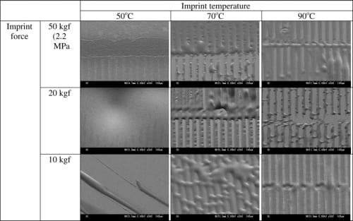
Fig. 4. SEM images showing thermal imprint test results with no pre-treated SU-8 samples. Collapse of imprinted pattern structures occurred due to viscoelastic deformation during and after de-molding.
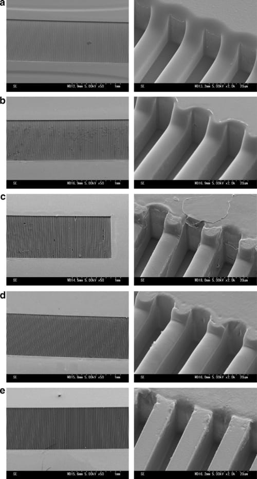
Fig. 5. SEM images of the imprinted SU-8 sample surfaces pre-treated with UV light for different exposure time (imprint conditions); (a) 30, (b) 20, (c) 15, (d) 10, and (e) 8 s.
Regarding the effect of O2 plasma, there still remains need for further study.
In Fig. 8, the process flow of an UV-assisted thermal imprint process and a conventional UV-imprint process of SU-8 was compared each other. Fig. 8a presents the process flow of the UV-assisted thermal imprint process, which involves surface pretreatment of un-cured SU-8 by UV exposure for few seconds, followed by thermal imprinting (90 °C). UV-exposure that performs prior to imprinting is the key sub-process and has a role in hardening the SU-8 surface to some extent. By short exposure to UV light (i line, 365 nm wavelength), strong acid (HSbF6) generates in a certain depth of a SU-8 surface layer. Generated SU-8 causes the epoxy resin to form a ladder-like structure with a high cross-linking density, cross linking reaction of SU-8 accelerated by heating during imprint procedure. Therefore, UV exposure conditions, imprint temperature and time are major process parameters that domains the replication fidelity. The balanced choice of the imprint temperature and the UV exposure condition is important because imprint temperature has reciprocal roles; the acceleration of cross-linking reaction and the reduction of material viscosity (within a certain temperature range). For examples, the SEM images of imprint SU-8 samples obtained under various combinations of imprint temperature and the UV exposure time are shown in Fig. 9. For given UV exposure conditions, the higher imprint temperature resulted in the better fidelity. Contrarily, increases of imprint temperature lead to two different results according to UV exposure c
onditions. For the imprint temperature of 90 °C, pattern fidelity decreased with increasing UV exposure time because a longer UV exposure time resulted in a higher cross-linked structure, thereby allowing for a harder surface. However, results for imprint temperature of 80 °C exhibited contrary tendency.
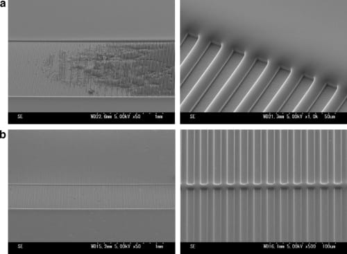
Fig. 6. SEM images of the imprinted SU-8 sample surfaces pre-treated by heating under the different heating temperatures (imprint conditions); (a) 160 and (b) 180 °C.
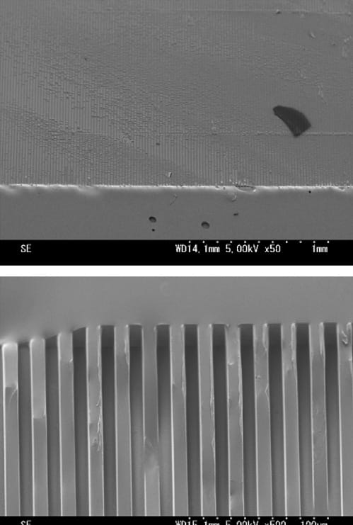
Fig. 7. SEM images of the imprinted SU-8 sample surfaces pre-treated by O2 plasma for 5 s (imprint conditions).
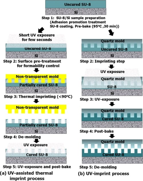
Fig. 8. Comparison of process flows between (a) an UV-assisted thermal imprint process and (b) a conventional UV-imprint process.
Fig. 10 shows several possible defects that can occur during the UV-assisted thermal imprint process. There were two types of defects including brittle fracture and the separation between the hardened surface and the un-hardened surface. Both defects occurred during mold releasing, indicating that an adequate mold release treatment is important
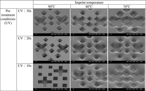
Fig. 9. SEM images of the SU-8 sample surfaces pre-treated with UV light for different exposure time imprinted under the same pressure and time at different temperatures (imprinting pressure, 2.2 MPa, imprinting time 300 s, and demolding temperature < 35 °C).
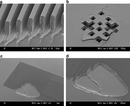
Fig. 10. SEM images of possible defects that occurred during UV-assisted thermal imprint process.
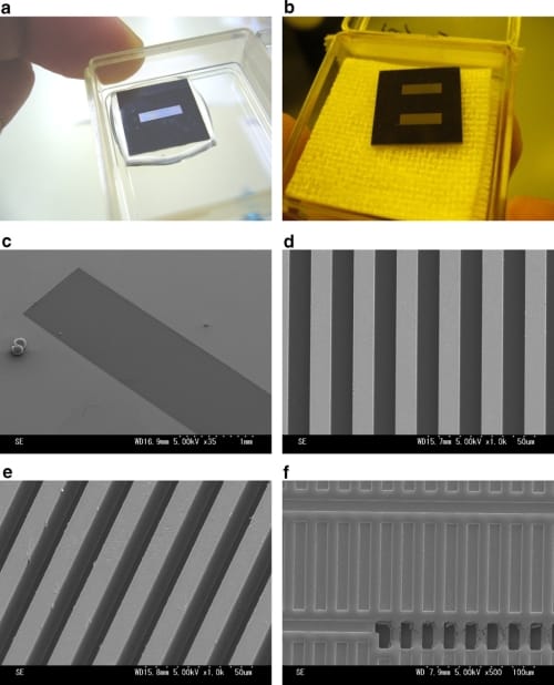
Fig. 11. SU-8/Si samples with micro pattern fabricated by thermal imprinting of the un-cured SU-8 resist pre-treated by UV light for 8 s; (a,b) Photographs, (c) SEM image of 200 arrays of 10 &um;m-wide and 1 mm-long lines with 10 &um;m spacing (aspect ratio: 2.5), (d,e) magnified SEM image of (c), (f) SEM image of 10 &um;m line-and-spacing pattern with 30 &um;m-deep via holes.
Fig. 11a represents the photographs of the imprinted SU-8/Si sample, and Fig. 11b–c show the images of the imprinted micro pattern in SU-8 resist. Complete filling of the un-cured SU-8, which was pre-treated by UV-exposure for 8 s, could be obtained under the following conditions: temperature, 90 °C; press force, 50 kgf (2.2 MPa); and imprinting time, 300 s. It could be observed that the features from the Ni mold are very well reproduced with good pattern fidelity. Please note that there may be different combinations of imprint parameters (e.g., temperature, pressure, presshead velocity, time, and UV exposure conditions).
As compared to conventional UV-imprint processes, this process showed three potential merits. The first is no need for a quartz mold, thereby allowing for the cost down of mold fabrication and the increase of applicable pattern dimension and geometry. The second and the third merits are an easier mold release and the less air-entrapment that are resulted from the hardened resist surface. The prevention of air entrapment is a crucial issue in the field of UV imprints [13].
5. Conclusions
In this study, we demonstrate the process to form a micro pattern in SU-8 film based on a thermal imprint process with nontransparent mold. Series of thermal imprinting tests using a Ni mold were performed with the un-cured SU-8/Si samples pre-treated by heating, UV exposure and O2 plasma, and their results were compared each other in terms of the replication quality. For the given imprint conditions and mold dimensions, a SU-8 sample pretreated with UV for 8 s resulted in the best replication quality. As a result, micro patterns could be successfully formed in high-heat resistant SU-8 resist at 90 °C by thermal imprint using a Ni mold.
As compared with conventional UV-imprint processes, this process has potential merits such as a lower mold cost, an easier mold release and a less air-entrapment. The potential advantages over the thermal imprint processes of heat-resistant polymers are a better layer-to-layer overlay accuracy, a less thermal residual stress, and a less degradation of mold surface coated with a mold release agent.
Acknowledgement
The part of this work was financially supported by Hirose Sensing Technology Co., Ltd. (HST, Japan). The authors would like to express their deep gratitude to HST. Also, the authors would like to thank Mrs. Kazumi Suda for her technical support regarding thermal- imprint process.
References
- R. Feng, R.J. Farris, J. Micromech. Microeng. 13 (2003) 80.
- B. Xu, Y.-K. Lee, Q. Jin, J. Zhao, C.-M. Ho, Sens. Actuat. A 132 (2006) 714.
- C.H. Lin, G.B. Lee, B.W. Chang, G.L. Chang, J. Micromech. Microeng. 12 (2002) 590.
- W. Hu, B. Yang, C. Peng, S.W. Pang, J. Vac. Sci. Technol. B 24 (5) (2006) 2225.
- X. Chang, L.J. Guo, Microeng. Eng. 71 (2004) 277.
- X. Wang, Y. Chen, S. Banu, H. Morgan, S. Fu, Z. Cui, Microeng. Eng. 84 (2007) 872.
- B. Vratzov, A. Fuchs, M. Lemme, W. Henschel, H. Kurz, J. Vac. Sci. Technol. B 21 (6) (2003) 2760.
- M. Otto, M. Bender, B. Hadam, B. Spangenberg, H. Kurz, Microeng. Eng. 57–58 (2004) 361.
- Y. Kurashima, M. Komuro, H. Hiroshima, J. Taniguchi, I. Miyamoto, Jpn. J. Appl. Phys. 42 (2003) 3871.
- W.J. Dauksher, N.V. Le, E.S. Ainley, K.J. Nordquist, K.A. Gehoski, S.R. Young, J.H. Baker, D. Convey, P.S. Mangat, Microeng. Eng. 83 (2006) 929.
- K. Nakamatsu, K. Watanabe, K. Tone, T. Katase, W. Hattori, Y. Ochiai, T. Matsuo, M. Sasago, H. Namatsu, K. Komuro, S. Matsui, Jpn. J. Appl. Phys. 43 (2004) 4050.
- G.M. Schmid, M.D. Stewart, J. Wetzel, F. Palmieri, J. Hao, Y. Nishimura, K. Jen, E.K. Kim, D.J. Resnick, J.A. Liddle, C.G. Willson, J. Vac. Sci. Technol. B 24 (3) (2006) 1283.
- H. Hiroshima, M. Komuro, N. Kasahara, Y. Kurashima, J. Taniguchi, Jpn. J. Appl. Phys. 42 (2003) 3849.