Yung-Pin Chen, Yuet-Ping Lee, Jer-Haur Chang, and Lon A. Wanga)
Photonics and Nano-Structure Laboratory, Department of Electrical Engineering and Graduate Institute of Photonics and Optoelectronics, National Taiwan University, Taipei 10617, Taiwan, Republic of China
a) Electronic mail: [email protected]
(Received 28 December 2007; accepted 15 July 2008; published 5 September 2008)
The authors report a new method for fabricating submicron gratings on curved substrates by combining thermoforming and nanoimprint technologies. A preshaping film was used to provide uniform pressure distribution throughout the whole concave substrate with the diameter of 60 mm and the radius of curvature of 92.5 mm. The concave glass could be resin coated uniformly by a conventional spin coater through the support of a soft holder. Either the preshaping film or the soft holder could be a buffer layer to prevent the curved glass from crumbling, which may result from high gas pressure during the imprint process. As for demonstration, a Rowland circle type concave grating with a period of 1.2 μm was made, and the measured first order reflectance was about 20% at various wavelengths. © 2008 American Vacuum Society. [DOI: 10.1116/1.2968702]
I. Introduction
The interest of fabricating submicron structures on nonplanar substrates has been growing, especially for optics and sensor applications. For example, a designed diffractive optical element (DOE) is fabricated on a concave lens surface.¹ Curved surfaces are difficult to pattern down to submicron scale using conventional photolithography since the depth of focus of a projection system is very limited and thus hardly applicable to pattern curved surfaces. Some other patterning methods were reported to overcome this barrier such as the writings by ruling engine,² x-ray Lithographie GalVanoformung Abformung,³ e-beam,4 holographic,5 direct laser beam,6 ion beam proximity,7 etc. However, all these methods are time consuming, complicated and expensive.
Previously Xia et al. used a polydimethylsiloxane (PDMS) mold to provide conformal contact on a curved surface for patterning.8 Choi and Park also used PDMS molds to imprint submicron structures onto cylinders.9 To enhance close contact and uniform pressure when imprinting large surfaces, Chang et al. used gas-pressuring mechanism to compress soft mold/substrate stack microstructures.10 The patterns of the soft mold could be replicated with high quality over an entire 12 in. resin-coated area. Cheng et al. used gasbag pressure mechanism to pattern submicron patterns onto a large concave substrate.11 Gao et al. developed an air cushion press process which employed a special gasbag to enclose the mold/substrate in a pressurized chamber.12
In this work, we report a quick, simple, and potentially economic method to fabricate a concave grating. Soft molds and a special gas-assisted pressuring scheme were used. In addition, the preshaping of sealing film and soft holder arrangements were found helpful in the imprinting of submicron structures on curved surfaces.
II. Experiment
To obtain a curved grating, we used a flexible plane grating mold to replicate on a curved surface. First, a planar grating was fabricated by interference lithography (IL) on a silicon wafer coated with photoresist. The nominal period, A, of the interference fringes is determined by the incident angle θ of two symmetrical beams and can be expressed as
A = λ ÷ θ’
where λ is the wavelength of the laser. Since IL requires a coherence light source, an argon ion laser with a lasing wavelength at 351 nm was used in the exposure system. The period of the interference fringes was 1.2 μm and the incident angle was 8.4°. The diameter of the grating area was 2 cm.
After IL process, we duplicated the grating structure by casting PDMS (SylgardTM 184, Dow Corning) at a mix weight ratio of 10:1. The formed mold was put on a vibration isolation table and cured at room temperature for one day and a PDMS replicate grating mold with a thickness of 2 mm was obtained. The advantages of using PDMS soft mold are that it is flexible and can eliminate the problem of sticking during detachment since PDMS has low surface energy. Next, a PDMS soft holder was cast on the convex side of the substrate. The curved substrate was a watch glass, which one of the curved surfaces is concave and the other is convex. This soft holder would be helpful in the follow-up processes.
Conventionally, a seal film was used to prevent leakage of the gas chamber during gas pressure nanoimprint. Since the substrate had a curved surface, a plane seal film was difficult to provide uniform pressure over the curved area. A preshapingfilm by matched-mold forming process can solve this problem. Figure 1 shows the thermoforming process of makinga preshaping plastic film for curved nanoimprint lithography (NIL). There is a thermoplastic film such as polyvinyl chloride (PVC) with a thickness of 200 μm to be placed between two matching male/female heated molds, which are then pressed to each other by an iron bulk (1.4 kg) put on the male mold to shape the PVC film for 2 min. A preshaping film was obtained after cooled down and released from the molds. When the PVC film was heated to 130 °C above the glass transition temperature (Tg=87 °C) of PVC, it could be shaped easily by pressuring the two matched male/female molds. These two matching molds were made by machined aluminum. The male one was matched with the concave curvature and the female one was matched with the convex curvature of the watch glass. The preshaping film was prepared for matching the curved glass surface which had a diameter of 60 mm and a radius of curvature of 92.5 mm. It is noted that a preshaping film plays an important role in the curved surface NIL and could be replicated quickly by thermoforming.

FIG. 1. Fabrication process of making a preshaping plastic film
to be used as a sealing film for curved NIL. Detailed
description can be found in the
text.
The next process step is to coat resin on the curved surface. Conventionally, resin was dip coated onto curved substrates, but the resultant thickness could not be controlled easily. However, we could spin coat UV curable epoxy resin, for example, SU-8 2010 (Microchem, Newton, MA), onto the concave surface of the watch glass by using the soft holder, as shown in Fig. 2. It was noted that the watch glass could be held firmly by the soft holder since it was flexible and well matched with the curved surface. Then the bottom surface of the soft holder was sucked by a spin coater. The soft holder could act as a buffer between the curved surface of the concave glass and the plane of the spin coater. The resin thickness was measured at various positions by a thin film thickness measurement instrument (TF-166, New Span Opto-Technology). The mean thickness was found to be 10.89 ± 0.20 μm, consistent with the datasheet of SU-8 2002-2025.
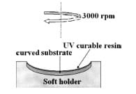
FIG. 2. Schematic illustration of spin coating the resin onto the curved
surface by using the soft holder.
Figure 3 shows the mechanism of the curved surface nanoimprint process. The soft holder, the resin-coated concave glass, the PDMS mold, and the preshaping film are placed in order in a vacuum chamber from the bottom up. When the PDMS soft mold put on the curved surface, it could match the curvature of the concave glass smoothly since PDMS was a flexible material. After the chamber was vacuumed and the substrate was heated to 95 °C, nitrogen (10 kgf/cm²) was introduced into the chamber to press the stacked substrate and the soft holder could prevent the curved glass from crumbling owing to gas pressuring. The PDMS soft holder was used to prevent the curved glass to contact rigid base directly in the chamber that would cause the glass crumbling during imprinting. The female aluminum mold covered with the preshaping plastic film could also be a buffer layer. Then, the photoresist was exposed to UV light for curing and cooled down by air. The exposure time was 5 min. The power of UV lamp (EA-140, Spectroline) was 800 μW/cm² for the wavelength ranging from 315 to 400 nm. Finally, the vacuum chamber was released to retrieve the imprinted substrate. The scanning electron microscopy (SEM) images of the interference photoresist gratings on a silicon wafer, the PDMS grating mold, and the imprinted SU-8 gratings on the concave glass are shown in Fig. 4. Their structures are very similar with the same dimensions.
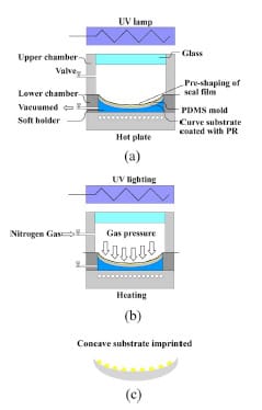
FIG. 3. Schematic showing the imprint principle for the
fabrication of a concave grating.
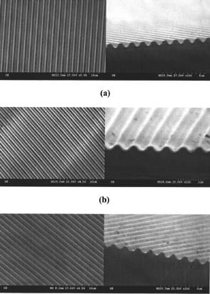
FIG. 4. SEM images of (a) the grating mother mold of the photoresist pattern,
(b) the PDMS mold, and (c) the imprinted SU-8 pattern.
The concave grating thus made could be used in a spectrometer. The main advantage is that a single concave reflective grating would combine both spectral splitting and focusing functions together, simplifying the arrangement. Since the resin and the glass had high transmittance, both were more than 85% in the range of the visible wavelength measured by utilizing the spectrophotometer (Hitachi-3501), we deposited a metal film, gold, with 30 nm to increase reflectance. The apparatus used to measure the spectral intensity of the concave reflective grating is shown in Figs. 5(a) and 5(b) where the letter is a schematic of this measurement system. By the geometry of the Rowland circle, light from a point light source on the circle plane was incident on a concave grating and the diffracted light would focus on the circle plane too. Thus the incident light and detector were located on the aerial Rowland circle. The concave reflective grating was placed on a rotation stage so that the incident angle could be varied. Furthermore the white light passed through a spatial filter to simulate a point light. The aperture stop was used to control the beam size of light on the concave grating to prevent the divergent light from being too large to exceed the grating area. A lens located on this focal plane was used to collect the diffracted light which was then guided by an optical fiber into a commercial spectrometer (HR4000, Ocean Optics) for analysis.
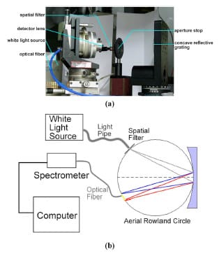
FIG. 5. (a) Photograph of the setup for characterizing the spectral responses
of a concave reflective grating and (b) a schematic of measurement system
for the spectral responses of a Rowland type reflective grating.
III. Experimental Results
The pressure distribution was measured by utilizing a pressure-sensitive film (LLW type, Fuji Prescale Film, Japan ). When the pressure was applied to the film, microcapsules were broken, generating distribution or “density” of magenta color which manifested itself the pressure distribution and magnitude. The color density of the pressed film was measured by using a densitometer detector (FPD305E/ 306E), and the uniform color density across the entire curved nanoimprinted field under the gas pressure of 20 kgf/cm² is shown in Fig. 6(a). The mean and standard deviation pressure magnitudes over the imprinted area were 19.6 and 0.80 kgf/cm², respectively. In contrast, the nonuniform pressure distribution was observed without using a preshaping film for sealing, as shown in Fig. 6(b). There were some wrinkles on the edges since the pressure was out of the range of the pressure-sensitive film (the maximum pressure sensitivity was 25 kgf/cm²) in these regions. This shows that the preshaping film can provide an excellent contact and enable uniform pressure over the whole curved area.
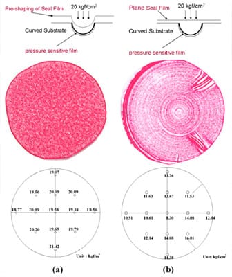
FIG. 6. Schematic showing pressure intensity distribution measurement.
Photos are (a)with and (b)without a preshaping film.
We also measured the optical transmittance of different material candidates for seal films and PDMS for mold in the UV wavelength range, as shown in Fig. 7. PDMS, PVC, and polyethylene terephthalate (PET) films showed good transmittance around the I-line range, and the shaded area of Fig. 7 indicates the process wavelengths for SU-8; therefore, they are suitable for UV NIL because optically they are relatively less lossy.
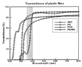
FIG. 7. Optical transmittance of PET, PC, PVC films, and
PDMS mold with thicknesses of 125 μm, 178 μm, 200 μm,
and 2 mm, respectively.
The photographs and SEM images of an imprinted concave grating are shown in Fig. 8. The diameter of the grating area was 20 mm and the grating period was 1.2 μm. Zeroth-, firs
t-, and second-order diffracted light beams were clearly observed on the screen. Furthermore the diffracted beams were focused along their propagating paths. Figure 9 shows different beam widths projected on the screen at different positions away from the concave reflective grating. The diffracted light indeed focused on the aerial circle plane and spread into a line with different wavelengths at different diffracted angles shown in position 2. This was consistent with our estimation from the Rowland circle geometry. Figure 10 shows the spectral intensity distributions of first and zeroth order. The incident angle was 24°. Moreover the collected lens was scanned on the aerial Rowland circle plane to measure the diffracted light spectrum. Since the focal plane was curved, the lens did not match the curvature. From this robust apparatus, the first-order reflectance at different wavelengths could be measured and was about 20% nearly as bright as the zeroth order. The reflectance is expected to be further improved by decreasing the grating period to prevent higher order diffracted light and by depositing a thicker metal film to increase the reflectance.
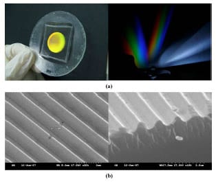
FIG. 8. (a) Photographs of an imprinted concave grating
on a dish and diffracted light and (b) SEM images of replicated
gratings with a period of 1.2 μm.
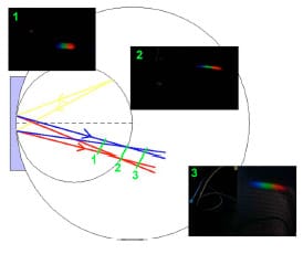
FIG. 9. Spectrograms of first-order diffraction at different locations.
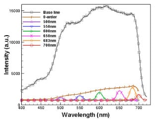
FIG. 10. Diffracted light intensity at different wavelengths.
The base line was the white light source spectrum.
IV. Conclusion
We present a simple and potentially cost-effective system by combining thermoforming and nanoimprint technologies to fabricate DOEs on curved substrates with submicron feature sizes. In addition to using gas-assisted pressuring scheme over a soft mold, we applied a preshaping film for sealing and a profile-matched soft holder to prevent the substrate from crumbling during the imprinting of submicron curved gratings. A concave reflective grating of Rowland circle fabricated by employing this technique was demonstrated and showed that the incident white light could be diffracted and focused to a curved plane.
Acknowledgments
The authors would like to thank ITRI and NSC for providing partial support for this work through Grant Nos. 7301XS7400 and NSC 95-221-E-002-325, respectively, and to ISIN Inc. for their assistance with pressure measurement.
References
- Y. J. Xie, Z. Q. A. Lu, F. Y. Li, J. L. Zhao, and Z. C. Weng, Opt. Express 10, 1043 (2002).
- T. Kita and T. Harada, Appl. Opt. 31, 1399 (1992).
- C. H. Ko, B. Y. Shew, M. C. Liang, C. C. Lui, and C. K. Lo, 2004 IEEE/LEOS International Conference on Optical MEMS and Their Applications (Optical MEMS 2004), Takamatsu, Kagawa, Japan, 2004 (unpublished), p. 136.
- D. W. Wilson, P. D. Maker, R. E. Muller, P. Z. Mouroulis, and J. Backlund, Proc. SPIE 5173, 115 (2003).
- E. Sokolova, B. Kruizinga, and I. Golubenko, Opt. Eng. (Bellingham) 2613 (2004).
- Y. J. Xie, Z. W. Lu, and F. Y. Li, Opt. Express 12, 1810 (2004).
- P. Ruchhoeft et al., J. Vac. Sci. Technol. B 17, 2965 (1999).
- Y. N. Xia, E. Kim, X. M. Zhao, J. A. Roger, M. Prentiss, and G. M. Whitesides, Science 273, 347 (1996).
- W. M. Choi and O. O. Park, Nanotechnology 15, 1767 (2004).
- J. H. Chang, F. S. Cheng, C. C. Chao, Y. C. Weng, S. Y. Yang, and L. A. Wang, J. Vac. Sci. Technol. A 23, 1687 (2005).
- F. S. Cheng, S. Y. Yang, S. C. Nian, and L. A. Wang, J. Vac. Sci. Technol. B 24, 1724 (2006).
- H. Gao, H. Tan, W. Zhang, K. Morton, and S. Y. Chou, Nano Lett. 6, 2438 (2006).


