Article: Chip Scale Review
Flip chip assembly electrically connects a face-down chip to a circuit board or substrate by microscopic conducting bumps of solder or pure metals. Accurate control of chip placement pressure and chip-to-substrate coplanarity is essential. Undetected pressure variations are a hidden cause of poor connections and non-coplanarity, reducing bonding yields and device performance. These pressure variations can be revealed and remedied by using pressure-indicating sensor film.
Bonders usually depend upon a force preset in a machine which is not capable of measuring pressure variations across the die. Some top-of-the line bonders provide laser measurements or optical auto-collimator measurements of coplanarity as expensive options. Pressure-indicating sensor film offers a viable solution for flip chip bonders to measure the pressure, or the uniformity of that pressure, across the die or bonding tool. A recent conference paper showed the advantages of a pressure-indicating film in wafer-to-wafer bonding.¹ Film may have similar advantages for several applications in flip chip assembly.
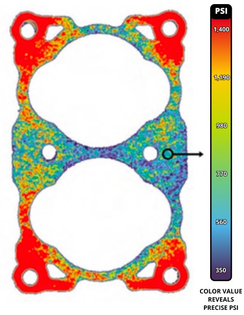
Placing pressure-indicating sensor film between two surfaces causes it to change color in direct proportion to the local pressure applied, giving an irreversible “pressure footprint” of the surface. Pressures over a wide range may be revealed with one vendor claiming 2-43,200 PSI (0.14-3,000 kg/cm²). The pressure magnitude at any point may easily be determined by comparing the color to a calibrated color correlation chart, analogous to using litmus paper to determine acidity. Figure 1 shows a color map of a wafer and its pressure interpretation. Visual comparison gives ± 10% accuracy in determining pressure. An optical measurement system increases accuracy to ± 2%.

Figure 1. Wafer pressure footprint and interpretation (courtesy Sensor Products Inc.)
The success of pressure-indicating sensor film in wafer bonding suggests similar applications in flip chip assembly, where pressure magnitude and spatial uniformity may be critical. This is particularly likely with large die, which are becoming more common. Die larger than 20mm², with more than 25,000 bumps per die, are already in routine production.² Potential pressure sensing applications include die-to-substrate coplanarity, bump coining for uniform bump heights, and several pressure-sensitive bonding methods..
Coplanarity
Successful flip chip assembly of large die with many bumps for applications such as image sensors depends upon the substrate, and the die that is being placed upon it, having parallel, coplanar surfaces when they are brought into contact. Any deviation from coplanarity can cause open or poor electrical connections. Extreme cases may misalign the die by imparting a sideways sliding motion during placement pressure, or may even crack the die. Figure 2 and Figure 3 show some potential effects of non-coplanar bonding.
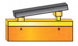
Figure 2. Misalignment may create acceptable bonds on side A but open circuits from failure to
bond on side B
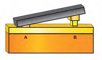
Figure 3. Misalignment may create short circuits on side A due to overpressure, and acceptable bonds
on side B
Conventional approaches for establishing and verifying coplanarity depend upon optical or laser equipment. However, most flip chip bonders do not have either of these expensive add-ons. Without them, establishing coplanarity often requires repeated trial-and-error planarity adjustments using sample assemblies and microscopic inspection.
Coining
Gold stud bump flip chip assembly places gold bumps on the die using a modified wire bonder. As deposited, those bumps have wire tails of varying length, as well as variations in bump height. Figure 4 shows a bump as deposited.
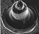
Figure 4. Gold stud bump showing wire stub at top
“Coining” by pressing the bumped die against a flat surface is a common method to reduce height variations and create larger contact areas. Figure 5 is a cross-section of a coined bump. When this is done, inadequate or non-uniform pressure across the die surface may cause some bumps to have varying heights, causing some open or poor contacts. Pressure-sensing film would verify uniform bump height.
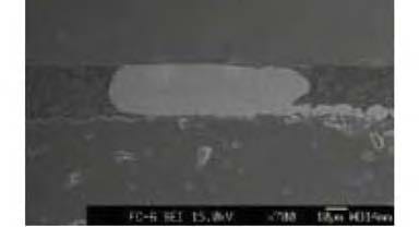
Figure 5. Cross section of a coined gold stud bump connection
Bonding
Many common methods of flip chip bonding require controlled, uniform pressure to avoid opens, poor contacts, and die cracking:
- Thermosonic bonding experiments found an optimum pressure for best bond adhesion. Higher or lower pressures gave poorer bond shear results.
- Thermocompression bonding requires higher bonding pressures than thermosonic, raising the consequences of inadequate pressure control. Copper/Copper thermocompression bonding of copper “nails” on a die to copper bond pads on a wafer has been demonstrated for high density 3D assemblies.
- Copper/Tin interdiffusion bonding of chips to wafers in 3D heterogeneous assemblies depends upon proper pressure at 300°C to form a stable copper-tin intermetallic, with copper upper and lower bonding surfaces.
- Gold/Tin wafer bonding tests show that too much pressure causes squeeze-out of solder, potentially leading to open or short circuits. Non-uniform pressure may squeeze solder out in some areas, but not in others.¹ The same problem could occur with large die in chip-to-substrate or chipto-wafer Gold/Tin bonding.
Common Assembly Problems
There are many common assembly problems associated with variations in pressure. Here are some common examples:
- Thermocompression bonding is used in both ordinary chip mounting and in 3-D die-onwafer assembly. Thermocompression flip chip squeezes adhesive out the sides and may cause die cracking.
- Indium bonding is used in flip chip assembly of large image sensor die that have thousands or tens of thousands of indium bumps connecting them to processor chips. Indium bumps self-weld on contact, so there are no second chances with a die that may cost thousands of dollars. Non-coplanarity on contact or non-uniform planar pressure can misalign the die or cause open or poor contacts, compromising the imaging performance of the sensor.
- Gold stud bumps for flip chip assembly are made with a modified wire bonder, which breaks the gold wire after attaching it to the chip leaving a small gold “stud.” Pressing a flat surface against the bumps gives uniform stud heights by compressing the randomheight wire stub left when the bond wire is broken. The uniformity of pressure ensures a higher probability of making all bump connections to the substrate, which saves time and money.
Conclusion
Flip chips minimize assembly size and improve electrical performance, making possible hand-held consumer products such as cell phones, cameras, calculators and iPods. More than 20 million wafers, each with thousands of chips, are forecast for flip chip bonding in 2010. The performance of pressure-indicating sensor film in wafer bonding and the importance of quality control in all of the above assembly examples suggest that film pressure sensing could significantly improve flip chip assembly yield, costs, and set-up time.
References
- D. Spicer et al, Pressure Indicating Film Characterization of Pressure Distribution in Eutectic Au/Sn Wafer-to-Wafer Bonding,International Wafer-Level Packaging Conference, pp. 135 – 139, October 27- 30, 2009.
- R. Asgari, Copper Pillar and Micro Bump Inspection Requirements and Challenges, Proceedings International Wafer-Level Packaging Conference, pp. 186 – 188, October 27 – 30, 2009.


