

Article
Related Links
Harutaka MEKARU and Masaharu TAKAHASHI
Advanced Manufacturing Research Institute, National Institute of Advanced Industrial Science and Technology (AIST), 1-2-1 Namiki, Tsukuba, Ibaraki 305-8564, Japan
Abstract
We have developed a new nanoimprint lithography (NIL) technology employing ultrasonic vibrations generated by a magnetostriction actuator where the process does not require any heating or use of ultraviolet light. In this work, a mold was mounted onto an upper loading stage using a negative-type resist. The mold pattern was then run through ‘‘push-into and pull-away’’ cycles on a molding material by applying longitudinal ultrasonic vibrations. For the molding material, poly(ethylene terephthalate) (PET) was selected because among engineering plastics its glass transition temperature is relatively low. Using this technique we succeeded in imprinting on PET at room temperature and made significant improvement in the throughput. The relationship between the depth of imprinted patterns and the contact force, or the contact time, was investigated by imprint experiments that employed an electroformed-Ni mold with convex patterns. The result of the experiment showed that, in working with ultrasonic NIL, the best contact force and the best contact time depend on the size of the pattern. The ultrasonic NIL technology has the potential of becoming a key technology for carrying out tasks on the scale of mass production.
Keywords: nanoimprint lithography, ultrasonic vibration, magnetostriction actuator, poly(ethylene terephthalate), room temperature
1. Introduction
Thermal nanoimprint lithography (NIL) technology was first proposed by Chou et al. in 1995.1) Since then, its applications in various fields have been studied and developed. When evaluating NIL as a viable manufacturing process, thermal NIL seemed to be the most promising candidate for manufacturing the next generation storage media such as Blue-ray discs. However, in order to establish thermal NIL as a technology for mass production it is necessary to minimize the cycle time in each process associated with the technology. Storage media such as the present compact discs (CD) and digital versatile discs (DVD) are manufactured mainly using injection molding technology. For this kind of work, polycarbonate (PC) is widely employed because of its good optical transmission and low water absorption properties. Currently, the processing time for manufacturing a single PC substrate by injection molding is about two seconds. We have been searching for newer technologies to improve the throughput in the thermal NIL. Currently two approaches are being pursued in this area. One approach is to incorporate an efficient heating mechanism into the thermal NIL system to shorten the heating time for the mold by accelerating the rate of temperature increase.2,3)
The other approach is to shorten the thermal cycle time by simply imprinting at low temperature. To pursue this approach we incorporated ultrasonic vibration into the thermal NIL technology. We had already succeeded in molding PC for which a heating cycle up to 180 °C (or beyond) was necessary. This temperature requirement has now been brought down to 160 °C by incorporating ultrasonic vibrations into NIL which resulted in the reduction of thermal cycle time by half.4) We also designed an experiment on NIL at room temperature where thermal cycling was not even required. For this experiment the piezoelectronic actuator of the existing ultrasonic vibration generator of the ultrasonic NIL system5–7) was replaced by a magnetostriction actuator. This change in the actuator mechanism impressed ultrasonic vibration of a higher magnitude than could be obtained by the earlier mechanism.
In an earlier paper, Lin et al. had reported on room temperature NIL using ultrasonic vibration. Using the piezoelectric actuator of a sandwiched transducer (Langevintype) 8) they were able to imprint on a Si substrate spincoated with a thermal-NIL resist mr-I 8030 (Micro Resist Technology, Tg ¼ 115 °C). In this case the Si mold was not mounted on an ultrasonic horn; rather the pattern side of the Si mold was in contact with the surface of the mr-I 8030 polymer spin-coated on a Si wafer. Afterwards, the ultrasonic horn was used to apply a pumping action on the backside of the Si mold by impressing an ultrasonic vibration as shown in steps 2 and 3 of Fig. 1(a). This operation imprinted nanopatterns at room temperature. The authors believe that imprinting at room temperature was possible because of the frictional heat generated by the ultrasonic vibration. To further study this phenomenon Lin et al. experimented with measurement of temperature rise with a built-in fine-wire thermocouple when an ultrasonic vibration is impressed on a stage. As a result, it was ascertained to rise up that the temperature rises to 100 °C in only 1 s after the ultrasonic vibration is initiated.9) On the other hand, our ultrasonic NIL method is shown in Fig. 1(b). In this case a mold is fixed on an ultrasonic horn. A negative resist was used as an adhesive for fixation as described below. Next, the mold was made to oscillate vertically so it could cycle through push (into the molding material) and pull (away from the molding material), as shown in positions 2 and 3 in Fig. 1(b). This technique proved to enable imprinting at room temperature by combining the repetition of a high-speed press and the frictional heating of plastic.
2. Ultrasonic NIL System using Magnetostriction Actuator
Figure 2(a) shows a photograph of an ultrasonic NIL system. This system comprises of a main device consisting of upper and bottom loading stages, a chiller system with coolant oil, and a computer for remote control operation. Figure 2(b) shows the region around the upper and bottom loading stages. The upper loading stage can be moved in a vertical direction with a servomotor for which the maximum loading force is 4.9 kN. The magnetostriction actuator selected for the experiment was AU-010N300-MS1 (ETREMA Product). Here, the frequency of the actuator could be varied from DC to 30 kHz with a maximum output and maximum amplitude of 720W and ±5 μm, respectively. Because the magnetostriction actuator generated heat when oscillating for a prolonged period, a water-cooled block connected with the chiller system was installed to cool the magnetostriction actuator. An electroformed-Ni mold was bonded to a 30-mm-square surface of an aluminum block with a negative ultraviolet (UV) resist (Toyo Gosei PAK-01) through a trapezoidal quartz plinth as shown in Fig. 3.10) The aluminum block is connected to the magnetostriction actuator in the upper loading stage with an M8 bolt. The center axis of the upper loading stage is supported at three points with micrometers that are installed above the magnetos
triction actuator. The aluminum block was horizontally placed at the bottom loading stage using a pressure measurement film (Fujifilm Prescale LLW) before a mold was bonded to it. After that, a PAK-01 resist was spread on both sides of the quartz plinth and a mold was bounded on one side. Using a servomotor the mold was lowered and made to gently touch the bottom loading stage. UV light was irradiated for 1 min using a UV-spot light source (Hamamatsu Photonics Photocure 200) from the other side of the quartz plinth. Using this method a mold could be fixed parallel to the bottom loading stage. A thermoplastic sheet was fixed to the bottom loading stage through a 3-mm-thick rubber sheet with a vacuum chuck.
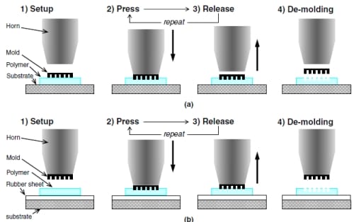
Fig. 1. (Color online) Process flows of ultrasonic NILs: (a) pumping-type ultrasonic NIL8) and (b) push-and-pull-type ultrasonic NIL.
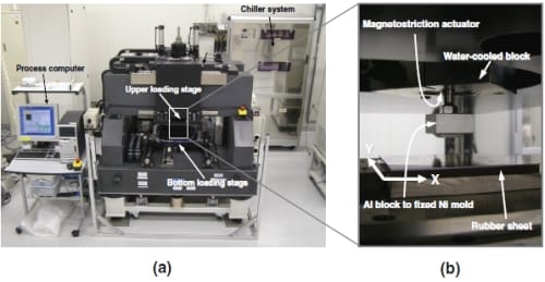
Fig. 2. (Color online) Photographs of (a) ultrasonic NIL system and (b) upper and bottom loading stages of ultrasonic NIL system.
3. Experimental Procedure
In the imprint experiment, an electroformed-Ni mold was used as a standard mold for a 15-mm-square cell by SCIVAX. Figure 4(a) shows an optical micrograph of the patterns on the mold. The line/space patterns in rows 1– 3 and dot patterns in rows 6 – 8 are of the convex-type 1 mm in height. The patterns in rows 4 and 5 (shown enclosed within a white frame I) are of the concave-type 1 μm in height. All these patterns are created in eight sizes: 500 nm, 700 nm, 1 mm, 2mm, 3mm, 4mm, 5mm, and 10 mm. The size of a mold pattern unit is 2 x 2mm2, and the same pattern units are arranged in a 5 x 5 matrix. The electroformed-Ni mold thus consists of a total of 25 units of mold pattern. The entire contact area of the mold pattern was about 27.4mm2 as estimated by calculation. Figure 5 shows scanning electron microscope (SEM) images of the line/space patterns on the electroformed-Ni mold with line widths of 500 nm, 700 nm, and 1 μm. These patterns appear inside the black frame II in Fig. 4(a). In the imprint experiment, three features of width 1 mm or less in the line/space patterns were selected for observation. No release agent of any kind was spread on the electroformed-Ni mold. The molding material selected was poly(ethylene terephthalate) (PET) (Tg: 75°C) because among engineering plastics its glass transition temperature is comparatively low. The PET sheet was 100mm square in area and 0.5mm thick.
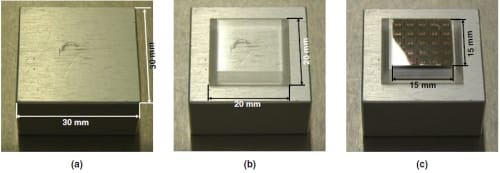
Fig. 3. (Color online) Setup procedure for electroformed-Ni mold on Al block.
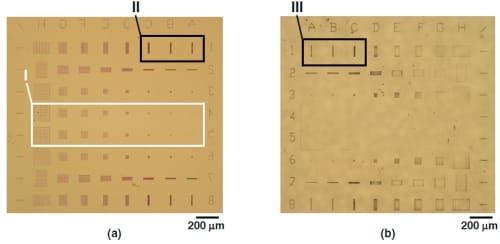
Fig. 4. (Color online) Optical micrograph of micro/nano-patterns on (a) electroformed-Ni mold and (b) PET sheet after imprinting.
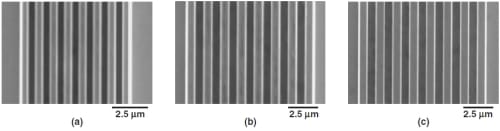
Fig. 5. SEM images of line/space patterns on electroformed-Ni mold for line widths of (a) 500 nm, (b) 700 nm, and (c) 1 μm.
4. Results and Discussion
In our conventional ultrasonic NIL experiments, a mold and a thermoplastic are heated up to a temperature in the vicinity of the glass transition temperature (Tg) of the thermoplastic. Then with the help of a loading force the pattern of the mold is pressed against the surface of the thermoplastic while at the same time a longitudinal ultrasonic vibration is impressed. At the end of the pressing cycle, the ultrasonic vibration is stopped and the cooling process is immediately started, which causes the thermoplastic to solidify. Finally, the mold is pulled away from the thermoplastic.11) However, in this study neither heating nor cooling of the mold or thermoplastic was involved. At first, the upper loading stage descended at a high speed of 10μm/s until the distance between the electroformed-Ni mold pattern side and the surface of the PET sheet reached 0.3 mm. After that, the mold was further lowered and pressed down at a reduced speed of 10 mm/s. The movement of the upper loading stage was stopped when it reached a set contact force where it was maintained for a set contact time. When the contact force reached its set value, the application of the ultrasonic vibration began, and the vibration continued for the set time. The upper loading stage was not moved although contact force changed during the duration of contact. Throughout the short duration, the frequency and the amplitude of the ultrasonic vibration were fixed at 10 kHz and 3 mm, respectively. The ultrasonic vibration was stopped after the contact time reached its set time, and then the upper loading stage was raised at a speed of 10 mm/s; during this step the electroformed-Ni mold was released from the PET sheet. Once the de-molding process was completed the speed of retraction switched to its previous high speed of 10mm/s, and the upper loading stage returned to its starting position.
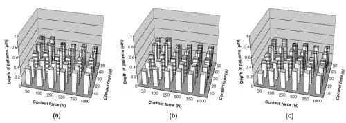
Fig. 6. Relation between contact force or contact time and imprinted pattern depth without ultrasonic vibration for line widths of (a) 500 nm, (b) 700 nm, and (c) 1 μm.
As a preliminary experiment in NIL, the imprinted pattern depth was investigated under conditions where pressure was applied but no ultrasonic vibration was involved. The depth of the pattern was measured using a five-line confocal microscope (Lasertec Optekics S130). The result of this experiment is shown in Fig. 6. It was possible to imprint on PET using only the loading force if the imprinted pattern depth were less than 0.5 mm. When the contact force was set at 50, 100, 250, 500, 750, or 1000 N, the expectation that the imprinted pattern depth would increase slightly with increasing force turned out to be the case only where the pattern width remained 1 μm or less. Moreover, in the experiment the contact time also varied and was set to 10, 20, 30, 60, or 90 s. The imprinted pattern depth became deeper accordingly with the contact force when the contact force was 50 and 100 N. However, when the contact force became 250N or more, any further variation in contact time showed no effect on the pattern depth. The contact force might cause a shift from elastic deformation to plastic deformation between 100 and 250N on the surface of PET, although it is considerably lower than the compressive strength of bulk PET (110–123 MPa).12) Such technique for molding a nanopattern only using pressure was proposed and referred as a direct nanoimprint technique by Yokoo et al.13)
The next experiment deals with the depth of the imprinted pattern when ultrasonic vibration was also applied, while using the same imprint conditions as in the previous case. The results are shown in Fig. 7. It has been understood that applying the ultrasonic vibration overall deepens the imprinted pattern. In general, it has also been understood that if the contact time became long, the imprinted pattern depth would become deeper. More frictional heat develops when the impressed time of the ultrasonic vibration is prolonged. The molding accuracy seems to have improved in ultrasonic NIL because the transformation by contact force was combined with the softening of the plastic by frictional heat. However, the best conditions for the contact force depend on the width of the pattern. The optimized contact force when the width of the pattern was 500 and 700 nm was 250 N; and when the width of the pattern was 1 μm,
the optimized force was 500 N. Specifically, it succeeded in a complete transcriptions of the 1-μm-wide imprinted pattern to a depth of 1 μm, where the optimized condition was a contact force of 500N and a contact time of 60 s. We believed that, because the ultrasonic vibration was held down, when the contact force grows too much, the effect of assistance of the ultrasonic vibration becomes obstructed. Figure 4(b) shows an optical micrograph of an imprinted pattern on PET where the ultrasonic NIL was executed under optimized conditions. It succeeded in imprinting all patterns except the convex pattern. Figure 8 shows SEM images of the line/space pattern of 500 nm, 700 nm, and 1 μm in the pattern width shown inside the black frame III in Fig. 4(b). The line/space patterns can be clearly distinguished in all patterns, and a sharp edge can be observed especially in the 700 nm and 1 μm width patterns.
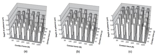
Fig. 7. Relation between contact fore or contact time and imprinted pattern depth with ultrasonic vibration for line widths of (a) 500 nm, (b) 700 nm, and (c) 1 μm.
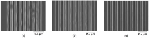
Fig. 8. SEM images of imprinted patterns on PET under optimized conditions for line widths of (a) 500 nm, (b) 700 nm, and (c) 1 μm.
Finally, the uniformity and reproducibility of the process in the case of optimized ultrasonic NIL conditions were investigated. Twenty five mold pattern units that contained a mix of concave and convex patterns of 200 x 200 mm2 were arranged as described in the foregoing paragraph. The imprinted patterns were measured at the center and four corners of the region of observation. Figure 9 shows the measured results of the pattern height of the electroformed- Ni mold before it was used. The uniformity can be confirmed for the 1-μm depth in each pattern of 500 nm, 700 nm, and 1 &um;m. Next, the patterns depth on PET, imprinted using optimized conditions, is shown in Fig. 10. The x- and y-axes in Figs. 9 and 10 indicate the direction of X and Y shown in Fig. 2(b). It was confirmed that the distribution was almost uniform. Moreover, after 50 continuous imprintings under optimized conditions, the samples of 1, 25, and the 50 shots were pulled out. Figure 11 shows the results of measuring the depth and width of patterns in these imprints. Data on the left in this figure is a result of measuring the depth and width of the pattern in the electroformed-Ni mold before it was used. The bar graph shows the pattern depth (height in case of the mold), where the values are shown along the left z-axis. Plots show the width of the line and the width of the space in the patterns, and those values can be read on the right z-axis. The width of the line is the width of the convex part in the electroformed-Ni mold and the width of the concave part in the imprinted pattern. The width of the line seemed to be decreasing by about 1–1.5% compared with the width of the space, although the 1-μm pattern height of the electroformed-Ni mold remains uniform. This tendency was observed on the imprinted patterns at widths of 500 and 700 nm. However, the width of the space became small, even more so than the width of the line at the pattern width of 1 μm. Because the imprinted pattern completely molded up to 1 μm in depth, there is the possibility of transforming it by the release force. Reproducibility is high from the overall viewpoint, although the first shot of the pattern width at 500 nm was small.
5. Conclusions
We developed a new ultrasonic NIL system equipped with a magnetostriction actuator. This magnetostriction actuator has a feature with which ultrasonic vibrations of large amplitude can be generated over a wide range of frequencies. By imprinting the pattern on an electroformed-Ni mold onto a PET sheet, the optimized conditions for the ultrasonic NIL system were explored. By keeping other conditions fixed, the contact force and contact time were varied and the effects of ultravibration on imprints were examined. As a result, the imprinted pattern depth at room temperature and without the use of ultrasonic vibration was found to be as deep as 0.5 mm. However, with a contact force of 500N and contact time of 60 s, the depth of the 1-μm-wide pattern reached 1 μm. Here we succeeded in a complete imprinting. By SEM observation, the edge of the line/space pattern was found to be well defined. Moreover, the pattern exhibited excellent uniformity when its distribution was investigated by measurements on the center and four corners of the region containing the pattern. The imprining also showed high reproducibility for 50 continuous shots when optimized conditions were used. Thus we showed that ultrasonic NIL with a magnetostriction actuator can be used even with PET for a process time of only 1 min, where PET happens to be a general engineering plastic rather than some special class of resist for the NIL. The possibility of greatly improved throughput was experimentally shown by a push-and-pull ultrasonic NIL technology at the room temperature.
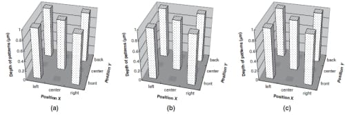
Fig. 9. Distribution of height of line/space patterns in electroformed-Ni mold for line widths of (a) 500 nm, (b) 700 nm, and (c) 1 μm.
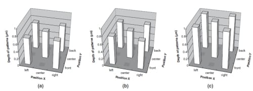
Fig. 10. Distribution of depth of line/space imprinted patterns on PET under optimized conditions for line widths of (a) 500 nm, (b) 700 nm, and (c) 1 μm.
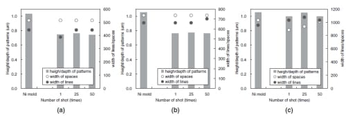
Fig. 11. Difference between depth and width of imprinted line/space patterns as functions of number of shots. Data on the left in the figure show the height and width of the mold patterns in the electroformed-Ni mold before it was used. The line/space width was designed as (a) 500 nm, (b) 700 nm, and (c) 1 mm.
Acknowledgment
We received valuable advice from Dr. Hiroshi Hiroshima of the Advanced Manufacturing Research Institute in AIST. We thank him for this advice and his cooperation.
References
- S. Y. Chou, P. R. Krauss, and P. J. Renstrom: Appl. Phys. Lett. 67 (1995) 3114.
- M. Takahashi, H. Goto, R. Maeda, and O. Maruyama: Proc. Japan. Society of Precision Engineering Conf., 2006, p. 737 [in Japanese].
- M. Takahashi, K. Sugimoto, and R. Maeda: Jpn. J. Appl. Phys. 44 (2005) 5600.
- H. Mekaru, O. Nakamura, O. Maruyama, R. Maeda, and T. Hattori: Microsyst. Technol. 13 (2007) 385.
- H. Kishi, H. Yoshioka, Y. Jianguo, N. Sumiyoshi, H. Goto, Y. Murakoshi, and R. Maeda: Proc. Nanoimprint Nanoprint Technology, 2003, p. 3.
- R. Maeda and K. Ashida: Seimitsu Kogaku Kaishi 70 (2004) 1219 [in Japanese].
- H. Mekaru, T. Noguchi, H. Goto, and M. Takahasi: to be published in Microsyst. Technol. (2008) [DOI:10.1007/s00542-007-0512-0].
- C. Lin and R. Chen: J. Microlithogr. Microfabr. Microsyst. 5 (2006) 011003.
- C. Lin, R. Chen, C. Su, and F. Chang: Proc. 2005 5th IEEE Conf. Nanotechnology, 2005, 0-7803-9199-3.
- H. Hiroshima: private communication.
- H. Mekaru, T. Noguchi, H. Goto, and M. Takahashi: Jpn. J. Appl. Phys. 46 (2007) 6355.
- Modern Plastic Encyclopedia Handbook, ed. Modern Plastic Magazine (McGraw-Hill, New York, 1973) Vol. 50, No. 10A, p. 534.
- A. Yokoo, M. Nakao, H. Yoshikawa, H. Masuda, and T. Tamamura: Jpn. J. Appl. Phys. 38 (1999) 7268.
![]()