Article: PLUS
Jeffrey G. Stark, President, Sensor Products Inc.
A recent conference paper [1] showed the advantages of a pressure-indicating sensor film [2] to establish uniform pressure across the wafers in wafer-to-wafer bonding. The extremely thin (4 to 8 mils) Mylar®-based film contains a layer of tiny microcapsules. Applying force to the Pressurex® film ruptures the microcapsules, immediately producing an image of pressure variations across the entire area. The colour intensity of the film varies at every point in direct proportion to the local pressure at that point.
Compressing the film between the plates of a wafer bonder produced an irreversible pressure footprint of the bonding surfaces. The amount of pressure applied at any point on the map is readily determined by comparing the colour at that point to a calibrated colour correlation chart. The colour comparison is analogous to that made when using litmus paper to determine acidity. Significant differences in bond pressure across the wafer bonder surfaces were revealed and corrected. Repeated pressure samples guided and verified the changes and adjustments made to achieve uniformity. The footprint was also scanned through imaging analysis equipment [3] to produce a multicolour pressure map.
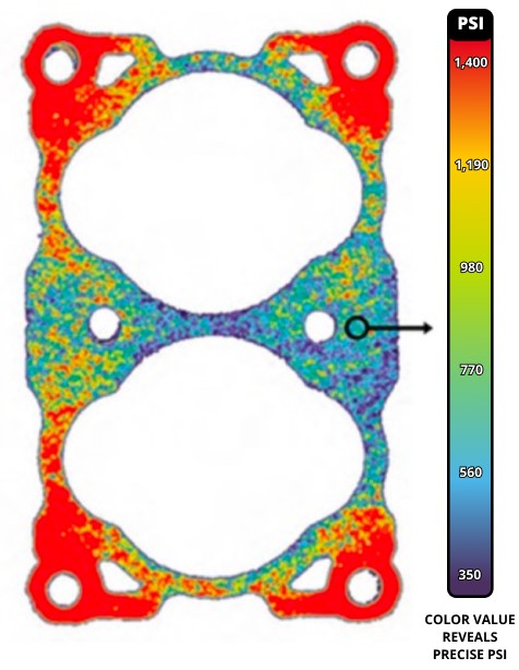
Figure 1 shows a typical colour map and its pressure interpretation. Visual comparison of a point to the colour correlation chart gives ±10 % accuracy in determining pressure. Imaging analysis increases accuracy to ±2 % and enables, a pressure profile as shown to be recorded and interpreted along any of the colour map. In many applications, the absolute pressure value is less important than relative pressure comparisons, which reveal non-uniform distributions of pressure over the area for correction. A post-correction map provides verification and a permanent record of pressure uniformity.
The success of pressure-indicating film in wafer bonding suggests that similar applications might be found in flip chip assembly, where both the magnitude and the spatial uniformity of applied pressure may be critical. This is increasingly important with the increasing trend towards larger die, which are becoming common. Die larger than 20 mm square are already in routine production [3].
![]()
Potential pressure sensing applications in flip chip assembly include establishing or verifying die-tosubstrate co-planarity, controlling the pressure applied to assure uniform bump heights, and optimizing a number of pressure-sensitive bonding methods. Flip chip bonding equipment in general does not directly measure or control pressure. Applied force is set in the machine, and an average distribution of total force over the contact area is assumed to represent pressure. This approach assumes that the force is uniform over the bonding surface. The wafer bonder tests showed that spatial non-uniformities of pressure, for example from tool wear, can be substantial – and can be corrected using pressure-indicating film.
Co-planarity
Successful flip chip assembly, especially of large diewith many bumps in applications such as image sensors, requires that the substrate and the die that is being placed upon it have parallel, co-planar surfaces when they are brought in contact. Any deviation from co-planarity may cause misalignment of the die with the substrate bond pads, resulting in open or poor electrical connections. Extreme cases of misalignment may cause a sideways sliding motion of the die during placement. Pressure differentials across the die may even crack the die. Figures 2 and 3 show some potential effects of non-coplanar bonding [4].
Conventional approaches for establishing and verifying co-planarity depend upon optical or laser equipment. The optical system establishes co-planarity by adjusting the tilt of one surface relative to the other until the images are aligned in an optical collimator. The laser system compares reflections from different locations while the die or wafer is tilted to establish co-planarity. Reflective gold spots must be added at several locations on the die or wafer for laser reflections. However, most flip chip bonders are not equipped with either of these expensive add-on accessories. Without them, manually establishing co-planarity often requires repeated trial-and-error adjustments to establish a common focal distance to several points on the die with a high-powered microscope. Multiple sample assemblies may be required for co-planarity verification.
Coining
Gold stud bump flip chip assembly places gold bumps on the die using a modified wire bonder. In normal wire bonding, the bonder makes a connection on a chip bond pad, and then extends the wire to make a second connection onto a substrate or package lead frame. In stud bumping, the wire bonder makes the first connection, and then breaks the wire.
| Figure 2. Misalignment may show acceptable bonds on side A, but create open circuits from failures to bond on side B, where the coplanarity error prevents the bumps from making contact with the pads | Figure 3. Another example of misalignment might create short circuits on side A, where excessive pressure compresses and spreads the burnp material to adjacent pads, while the bumps on side B may still show acceptable bonds. |
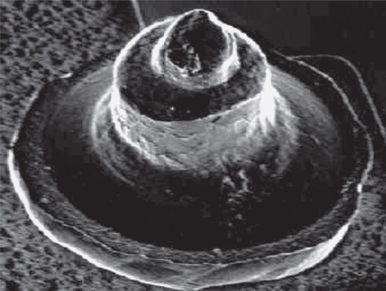
First, a small gold sphere formed by melting wire at the wire tip is metallurgical bonded to a chip bond pad by heat, pressure, and sonic energy. The bonding tool next clamps on the wire, and pulls it to break the wire somewhere near the bump. The tool then moves to the next bump location, creates a new ball by melting the end of the wire with spark or electric flame-off as in normal wire bonding, and repeats the bump placement sequence on another bond pad. The bumps as deposited have wire tails of varying length, and the bumps themselves may vary in height. Figure 4 shows a bump as deposited.
 | |
| Fig. 4: In this gold stud bump, the gold ball has been pressed flat on the bond pad, with the wire stub protruding from the top of the bump | Fig. 5: Cross-section of a gold stud bump, with the top surface flattened by pressure |
Stud bumps may be coined by pressing the bumped die against a flat surface as a simple method to reduce height variations and create larger contact areas. Figure 5 shows a crosssection of a coined bump. Again, inadequate or nonuniform coining pressure across the die surface may cause some bumps to have height differences, leading to open or poor contacts. Pressure-indicating film could be applied to verify uniform bump heights after coining.
Bonding
Many common methods of flip chip bonding require controlled, uniform pressure to avoid open contacts, poor contacts, and die cracking:
- Thermo sonic stud bump bonding experiments determined that there is an optimum pressure for maximum bond adhesion. Bonding pressure was varied across a range from 40 grams to 100 grams per bump. Die shear measurements demonstrated that bump adhesion to the bond pad at the optimum placement pressure was more than 40 % greater than at the extremes [4]
- Thermo compression bonding requires higher bonding pressures than thermo sonic bonding, raising the hazards of inadequate pressure control. Copper/Copper thermo compression bonding of copper nails on a die to copper bond pads on a wafer has been demonstrated for high density 3D assemblies [5]
- Copper/Tin interdiffusion bonding of chips to wafers in 3D heterogeneous assemblies depends upon proper pressure at 300 °C to form a stable coppertin intermetallic, with copper upper and lower bonding surfaces [6]
- Gold/Tin wafer bonding tests show that too much pressure sometimes causes squeeze-out of solder, potentially leading to open or short circuits. Nonuniform pressure may squeeze solder out in some areas, but not in others [1]. A similar problem could occur with large die in chip-to-substrate or chip-towafer Gold/Tin bonding.
While published papers may not have yet reported the results of using pressure-indicating film for controlling flip chip assembly pressure uniformity, the importance of control in all of the above examples suggests that pressure indicating film might significantly improve yield, costs, and set-up time.
About Jeffrey G. Stark
Jeffrey G. Stark founded Sensor Products Inc. in 1990 to meet what he thought would become a growing need for pressure indicating sensors that could profile the force distribution between two contacting objects. The company continues to devote itself to providing customized sensor solutions as well as uniform products that meet the needs of a diverse clientele.
About George A. Riley, PhD
George A. Riley has more than 20 years experience in microelectronics packaging, including 10 years developing and manufacturing flip chip assemblies for more than 50 customers. He is an industry consultant, educator, and web entrepreneur who has authored more than 90 papers and articles. He can be reached at (508) 753-3572, by emailing [email protected] or by visiting his website www.flipchips.com
Reference
- D. Spicer et al, Pressure Indicating Film Characterization of Pressure Distribution in Eutectic Au/Sn Wafer-to-Wafer Bonding, Proceedings International Wafer-Level Packaging Conference, pp. 135-139, October 27-30, 2009
- Sensor Products Inc. Pressurex® Film, www.sensorprod.com
- R. Asgari, Copper Pillar and Micro Bump Inspection Requirements and Challenges, Proceedings International Wafer-Level Packaging Conference, pp. 186-188, October 27-30, 2009
- L. K. Cheah et al, Gold to Gold Thermosonic Flip-Chip Bonding, Proceedings HDI 2001, April 2001, pp 165-175. See also www.flipchips. com/tutorial09.html
- P. De Moor et al, Recent Advances in 3D Integrations at IMEC, MRS Fall Meeting, November 27-December 1, 2006, Boston MA. See also www.flipchips.com/tutorial71.html
- M. Jurgen Wolfe et al, Technologies for 3D Heterogeneous Integration, Proceedings of SMTA Pan Pacific Symposium 2008. See also www.flipchips.com/tutorial90.html


