Article: DPAonthenet.net

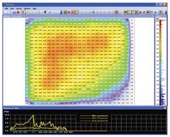
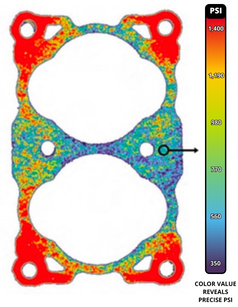
With Tactilus®, engineers can visualise actual contact forces and pressure distribution data on the circuit board components. As the mounting screws between the CPU and the heat sink are tightened, Tactilus® maps and measures the changing pressure distribution between the mating surfaces and displays it on-screen. The heat sink interface can be tested, manipulated, and repositioned in real-time, speeding the trial and error process and eliminating the need for additional assembly. Tactilus® also provides the pressure data needed for FEA simulation predictions.
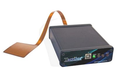
Unlike conventional transducers, the Tactilus® sensor is flexible and only 0.38mm thick, so it can be placed between the CPU and heat sink without affecting the assembly. The sensor pad has 625 resistive sensing points arrayed on a 25 × 25 grid, providing a total sensing area of 50 x 50mm. The scan speed is up to 1,000Hz, and the operating pressure range is 0 to 7 kg/cm2.

Tactilus® collects and processes sensor data using easy-to-use, Windows-based software that performs the following tasks:
- Creates pressure vs time graphs and histograms;
- Performs 2D, 3D and 360 degree image rendering and region of interest scaling;
- Displays maximum, minimum, and average pressures and does force integrations; and
- Prepares reports through export to Excel, ASCII, or Access formats.
The Tactilus® sensor system will endure hundreds of diagnostic uses on different heat sinks with consistent repeatability. It is highly resistant to electromagnetic noise, temperature variation, and humidity fluctuations. Accuracy is ± 10%; repeatability is ± 2%; hysteresis is ± 5%; and non-linearity is ± 1.5%. The system can also be used to map and measure surface pressure distribution at the interface of tyre tread footprints, door seals, heat seals, fuel cells, printed circuit boards, flat panel displays and wafer polishing, among others.


