


Withstanding the Pressure: How to pre-stress your press-pack power semiconductors
To achieve optimum performance of press-pack power semiconductors, they must be mechanically clamped in a precise manner. This article explains a technique to verify that the pressure distribution is homogenous and the magnitude is appropriate during the design of the assembly.
Press-pack high power semiconductors are in many applications very powerful components in controlling electrical power. To utilize their full potential, a proper mechanical design of the complete assembly, including press-pack high power semiconductors, heat sinks, bus bars and other components, is crucial. This article addresses some important issues for the mechanical design and the assembly work for stacks using presspack high power semiconductors and also shows how the pressure distribution can be verified using Fujifilm Prescale® film.
Interface properties
The current and heat conducting interfaces should be designed to retain good conduction properties throughout the equipment lifetime. This is accomplished by creating a sufficient number of stable metal-to-metal connections, referred to as “a-spots” in contact theory, which can efficiently conduct current from the semiconductor through the heat sink to the bus bars. These a-spots must be maintained during high stress conditions such as load cycling, vibration and chemical contamination such as exposure to sulphur gases. To achieve this, care must be taken in choosing the right materials for the components, which must be coated properly and have the right surface finish. Since the most critical interface is between the press-pack high power semiconductor and the heat sink, we will focus on this interface.
Surface finish and treatment are crucial processes for optimal heat and current conduction over the device and heat sink interface. Press-pack high power semiconductors usually have a surface roughness Ra about 0.8 µm and flatness below 10 or 15 µm depending on pole piece size. It is recommended that the heat-sink surfaces have the same flatness and roughness as the presspack high power semiconductor measured on the surface where the device is to be mounted.
The use of heat sinks with a good quality plating of nickel or silver is recommended… Bare copper or aluminum is not recommended due to corrosion that rapidly deteriorates the contact surfaces. Although nickel and silver do corrode, the nickel and silver oxide do not deteriorate the interface to the same extent as aluminum oxide. Often press-pack high power semiconductors have pole pieces of copper with a nickel-plating of approximately 5 µm. For nickel-plated devices it is recommended to use the same plating thickness on the heat-sink area that is in contact with the device. For applications with hard component stress, it is recommended to use chemical plating when the semiconductor is electrolytically plated or vice versa.
Mechanical design
The clamping must be carefully designed to ensure that the device is clamped with the right force and it must also allow homogeneous pressure distribution over the whole contact surface of the device. Uneven pressure will lead to deformation of the housing and internal stress between the different layers inside the device, causing it to fail prematurely during load cycling. Designing for pressure uniformity is not always easy, and the complexity should not be underestimated. Simple solutions, such as clamping the device between two rectangular plates by bolting down the corners will result in poor reliability.
Ideally, the mounting force should be applied from a single point above the centre of the device. Our recommendation is that the centre of the force is within 2 mm from the centre of the device, and at a minimum distance equal to half the pole-piece diameter of the device measured from the device surface, as shown in Figure 1, to achieve a good pressure uniformity considering the “90° force cone”. A spherical cup between the mounting clamp and the pressure spreader above the heat-sink can act as this single point of force and ensures that the force from the mounting clamp is transferred symmetrically to the device. It also allows parts within the stack to adapt to inherently present non-parallelisms. There will always be inherent non-parallelisms in a stack since it is not possible to manufacture heat sinks and press-pack high power semiconductors with perfectly parallel surfaces, but the non-parallelisms should be reduced as much as possible. The non-parallelism between the anode and cathode pole pieces is normally = 100 µm for devices with a pole piece diameter = 50 mm and = 150 µm for devices with a pole piece diameter > 50 mm.
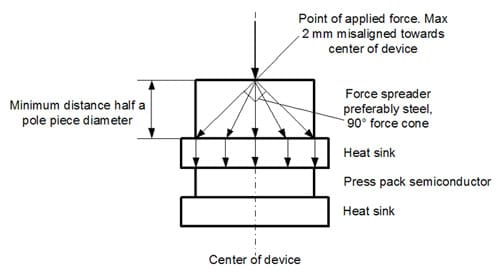
Figure 1: Force spread cone
The components and the clamp design must be chosen to withstand temperature levels and forces caused by mechanical expansions and contractions due to temperature changes that occur during working conditions, to prevent damage over the whole equipment lifetime. The design must also allow for temperature expansion and contraction without large changes in force and pressure distribution on the press-pack high power semiconductor.
Press-pack high power semiconductors, whether parallel or anti-parallel connected, should always be clamped separately as shown in Figure 2. Due to mechanical tolerances there will be differences in height and parallelism that in many cases will create mechanical forces large enough to significantly reduce the lifetime or even destroy the devices if two or more devices are clamped together between two rigid bus bars or heat sinks.
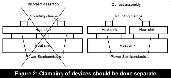
Figure 2: Clamping of devices should be done separate
If several devices are assembled together in one stack with the same mounting clamp, they must have the same rated mounting force. This is to avoid over-stress or too low pressure for some of the devices in the stack. It is also advisable to use devices with the same pole piece diameter to simplify the heat-sink design in order to achieve good pressure distribution on all devices. If the heat sink cannot spread the pressure evenly and devices with different pole piece diameters are used, there is a high risk that either the rim of the smaller device will get too high pressure or the rim of the large device will get too low pressure. An example of a well-dimensioned stack is shown in Figure 3. Figure 4 shows a badly designed stack using only thin force spreaders and insufficient heat sinks that do not spread the force evenly over devices with different diameters. Stacks with different device diameters can be made, but only with welldesigned heat sinks and force spreaders to ensure a homogeneous pressure distribution.
Verification of the pressure distribution
To verify that the pressure distribution is uniform, we recommend the use of Fujifilm Prescale® tactile pressure indicating sensor film or similar products.
The first verification step is to mount the stack according to standard procedures with pressure films between the semiconductor and the heat sink on both sides of the semiconductor. For a good result, it is important to follow the instructions from the film manufacturer and make sure that the right film grade is used. If the result is good, no further investigation is normally needed. If the result is bad, the next step is to apply a pressure film on the other interfaces in the stack, as between the heat sink and bus bar or between the heat sink and force spreader. This gives the complete picture of the force distribution within the stack, thus enabling tracking of the weak point in the system that needs to be improved to get good force distribution on the power semiconductor.
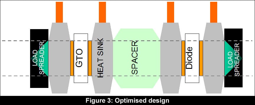
Figure 3: Optimised design
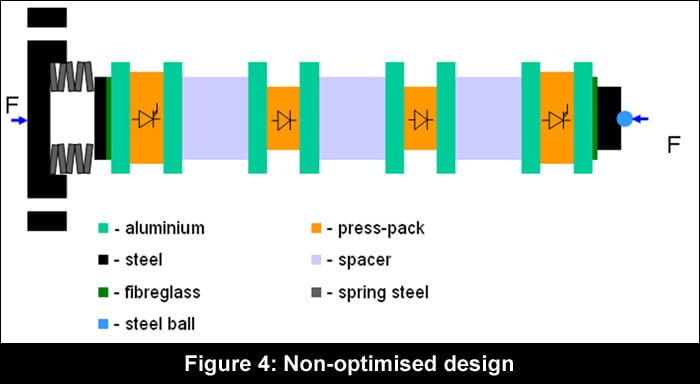
Figure 4: Non-optimised design
Figures 5 and 6 show two samples from pressure distribution measurements on IGCT’s with Fujifilm Prescale® film. Figure 5 shows good pressure distribution and figure 6 shows poor pressure distribution, with a large area of the device having too low pressure and some areas having to high pressure.
Seldom are the cases clearcut. There are unfortunately no simple rules that predict whether a mechanical design will be good enough for its intended purpose. Experience is normally the only way to determine if a design is good enough for its purpose or not.
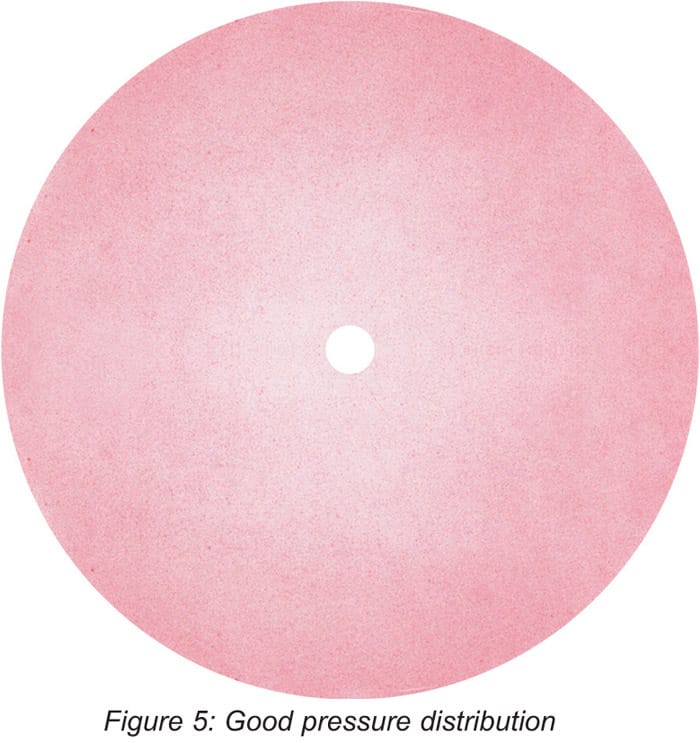
Figure 5: Good pressure distribution
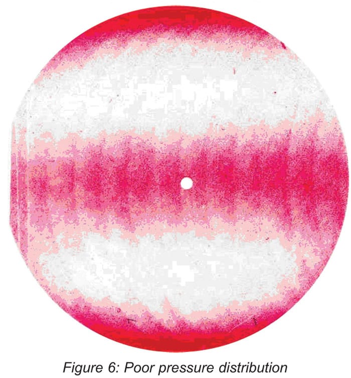
Figure 6: Poor pressure distribution
Advanced verification of the pressure distribution
In addition to the simple visual investigation of the pressure film, there are more sophisticated analysis tools available such as the Topaq®.
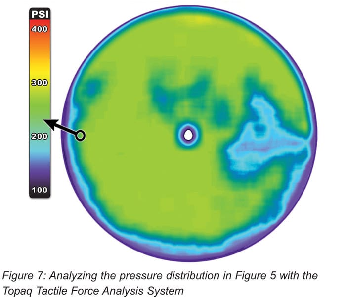
Figure 7: Analyzing the pressure distribution in Figure 5 with the Topaq Tactile Force Analysis System
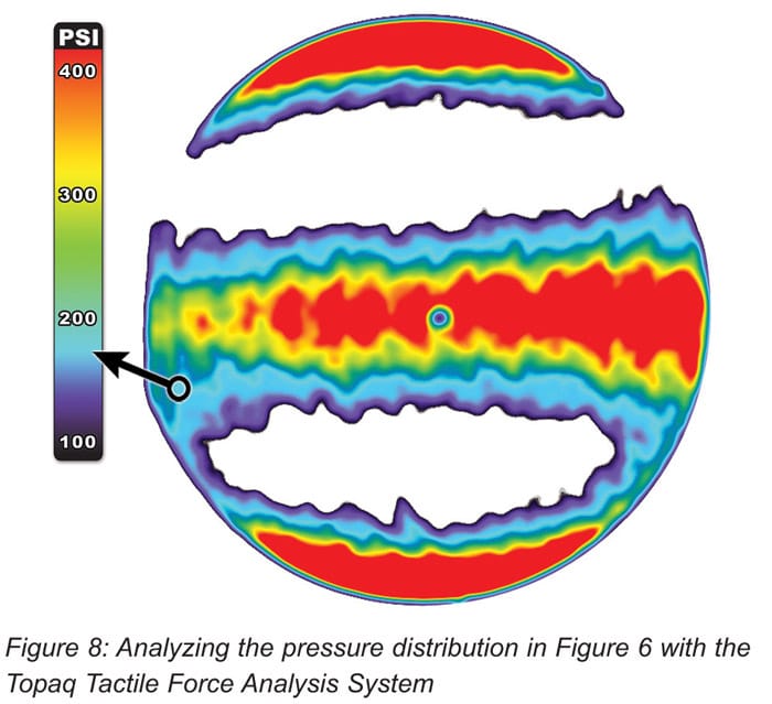
Figure 8: Analyzing the pressure distribution in Figure 6 with the Topaq Tactile Force Analysis System
With this tool, the various shades of red that show pressure distribution on the film are presented in a wider range of colors, giving a highly-detailed statistical picture of the pressure distribution. When analyzing the examples from figures 5 and 6, we get the following results:
As can be seen, the homogeneity in figure 5 is not as good as first thought, although it is for practical purposes good enough. For figure 8, we see that the spread in pressure distribution is large and that further measures are needed to improve the situation before the equipment using this semiconductor goes into operation.
Written by Björn Backlund, ABB Switzerland Ltd, Semiconductors and Jeffrey Stark, Sensor Products Inc. (USA)
| Pressure Film Type | Code | Alternative Code | Pressure Range | Order Now |
| Ultra Extreme Low | 5LW | UXL310 | 0.87 – 7.3 PSI (0.06 – 0.51 kg/cm2) | Order Now |
| Extreme Low | LLLLW / 4LW | XL310 | 7.2 – 28 PSI (0.5 – 2 kg/cm2) | Order Now |
| Ultra Low | LLLW | UL270 | 28 – 85 PSI (2 – 6 kg/cm2) | Order Now |
| Super Low | LLW | SL270 | 70 – 350 PSI (5 – 25 kg/cm2) | Order Now |
| Low | LW | L270 | 350 – 1,400 PSI (25 – 100 kg/cm2) | Order Now |
| Medium | MS | M270 | 1,400 – 7,100 PSI (100 – 500 kg/cm2) | Order Now |
| High | HS | H270 | 7,100 – 18,500 PSI (500 – 1,300 kg/cm2) | Order Now |
| Super High | HHS | SH270 | 18,500 – 43,200 PSI (1,300 – 3,000 kg/cm2) | Order Now |
| Physical Specifications | |
| Operating Temperature | 68°F – 95°F (20°C – 35°C) much higher for brief exposure |
| Humidity Range | 20% to 90% RH |
| Gauge (Thickness) | 4 – 20 mils |
| Spatial Resolution | From 5 – 15 microns |
| Substrate | Polyethylene Terephthalate (PET) |
| Accuracy | ± 10% visual, ± 2% Utilizing optional optical measurement systems |
| Shelf Life | 1 Year |