Article
Related Links
A dissertation submitted to the Division of Graduate Studies and Research of the University of Cincinnati in partial fulfillment of the requirements for the degree of Doctorate of Philosophy in the Department of Electrical & Computer Engineering of the College of Engineering Dec 2008
By Yaling Zhou
B.S. Electrical Engineering, Southeast University, China, 2001
Thesis Committee:
Joseph Boyd, PhD
Thomas Mantei, PhD
Jason C. Heikenfeld, PhD
Jan M. Yarrison-Rice, PhD
Committee Chair: David Klotzkin, Ph.D
Bonding Process
Unlike 1-D and 2-D PhCs, 3-D PhCs require the periodic arrangement of materials with different dielectric constant in all three dimensions. With available microfabrication techniques, it is relatively straightforward to realize the periodic structure (gratings) in the x-y plane; the major challenge to repeat the same periodic structure in z direction, even with the simplest case of 3-D PhCs-woodpile structure. To stack the periodic structure layer by layer, a thermal compression bonding-technique for tungsten is developed and adopted. Previous work[98, 99], as demonstrated successful wafer-level thermal-compression bonds using Au. This is, to our knowledge, the first demonstration of thermal compression bonding with tungsten.
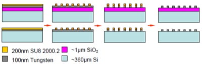
Figure 4. 10: Fabrication of Tungsten grating
The details of the bonding process are illustrated in Figure 4.9. A silicon wafer substrate and a silicon dioxide-on-silicon wafer substrate, each with around a cm2 with of patterned tungsten, are placed together with the tungsten wires oriented orthogonally and in intimate contact. They are mounted between two graphite pieces and loaded in a bonding clamp apparatus consisting of two stainless steel plates with four bolt holes drilled around the perimeter. The two stainless steel plates are tightened together through torqueing the bolts to a fixed value around 35 inch-lbs.
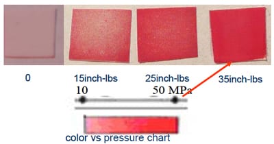
Figure 4. 11: Pressure sensitive film showing measurement and uniformity of bonding pressure. The actual pressure used is about 50MPa
To optimize the process and bonding parameters, including bonding pressure uniformity, the measured pressure between two bonded pieces is visualized by pressure measuring film as shown in Fig 4.11. The film is placed between two layers of Si and the fixture torqued to a particular value with the color of the film indicates the pressure experienced. Our initial bonding pressure is around 50 MPa. The apparatus with bonding pieces (Fig. 4.12(a)) inside is placed in a furnace in a nitrogen atmosphere. The furnace was gradually warmed up (50 degrees every 30 minutes) to 750 C, held there for 1-6 hours, and then stepped down. During the heating process inside the furnace, the actual pressure applied on the samples is increased due to the thermal expansion of the fixture. When cool, the pieces were removed. Figure 4.12(b) shows the top view and the cross section of two bonded pieces. Strong bonding between the pieces was observed. For further characterization of the process, samples were bonded with the same initial force of 50MPa and kept in the furnace for varying times. They were then removed from the furnace and the stress at failure was measured through destructive tensile testing. Figure 4.13(a) shows the time vs, force profile during destructive strength testing, indicating failure at a force of around 35kgF. Figure 4.13(b) shows the failure stress vs. bonding time for these samples. The bonding strength increased monotonically with bonding time and ranged from 2 to 9MPa.
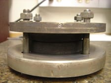
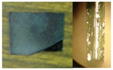
Figure 4. 12: (a) Wafer bonding chuck, showing two pieces of W-coated Si
sandwiched between two pieces of W clamped by screws (b) bonded W on Si, showing
center) top view, (right) side view
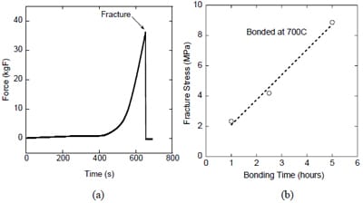
Figure 4. 13: (a) shows the time vs. force profile during destructive strength testing; the bond between the tungsten failed at about t=650s. (b) failure stress is characterized vs. bonding time at high temperature
Half Wafer Removal
After successfully bonding patterned tungsten, one substrate needs to be removed to uncover the stacked W wires in between and expose them for further bonding.