Article
Related Links
H. Hocheng*, T.T. Wen
Department of Power Mechanical Engineering,
National Tsing Hua University, Hsinchu 300, Taiwan, ROC
* Corresponding author: E-mail address: [email protected]
Abstract
Purpose: To develop methods for uniform imprint of micron and submicron-scale features.
Design/methodology/approach: The first is gas-assisted imprint technique. In use of gas to exert isotropic pressure in hot embossing, uniform embossing throughout the area is achieved. Another approach is the electromagnetic force-assisted imprinting technology, which employs the electromagnetic force to pull the magnetic stamp with submicron-scale structures into a UV-curable resist on the substrate. The liquid photopolymer is then cured by UV-irradiation at room temperature. Furthermore, the ferromagnetic UV-curable material is made of nano-Fe powder and UV-curable polymer. The micron and submicron-scale magnetic features can be fabricated.
Findings: Uniform embossing throughout the area is achieved. Under the condition of 180°C, 40kgf/cm2 and 90 seconds, high quality and uniformity of micro-optical components can be fabricated. For electromagnetic force-assisted imprinting technology, a large area of sub-micron pattern with a line width of 502nm and a pitch of 1um can be successfully fabricated under the condition of pressure of 1.6kgf/cm2 for 30 seconds and UV curing for 0.5 minute. Using ferromagnetic UV-curable resist, the structures can be successfully fabricated under the pressure of 0.92kgf/cm2 with the same UV-curable time. These results indicate good uniformity and controllability on both the gas-assisted hot embossing and electromagnetic force-assisted imprinting for efficient fabrication of micron- or submicron-scale structures.
Practical implications: The facilities have been designed, constructed and tested. The effects of processing parameters including the processing temperature, pressure, and time on the replication quality were investigated.
Originality/value: There are advantages of high uniformity, low pressure and low temperature for various applications in micron and sub-micron features and other micro-optical components such as gratings and waveguides etc.
Keywords: Plastic forming; Submicron-scaleimprint; Gas-Assisted; Magnetic force
1. Introduction
The polymeric micro- and nanostructure has been widely used in various fields such as optoelectronics systems, sensing devices and biomedical engineering etc. The ability to replicate patterns at the micro- to the nanoscale is of crucial importance to the advance of micro- and nano-technologies.
Nanoimprint is a novel lithographic technology that promises high-throughput patterning of micro and nanostructures with low cost. Based on the mechanical embossing principle, nanoimprint technique can achieve pattern resolutions beyond the limitations set by the light diffractions or beam scatterings in other conventional techniques. In recent years, there are several methods for imprint technologies developed. The examples are nanoimprint lithography, step-and-flash imprint lithography (SFIL) and soft lithography. The conventional nanoimprint technology is a hot embossing process [1-5], which involves temperature cycling and high pressure processing. It is very time-consuming. The step-and-flash imprint lithography (SFIL) uses UV-curable resist and employs UV light to cure the photo-polymer at low pressure and room temperature. However, this procedure requires transparent quartz stamps that apply a complex fabrication process and can be more expensive than the usual rigid stamps [6-8]. On the other hand, the soft lithography processes utilize soft PDMS stamp and low viscosity resists, allowing short process cycle and accurate structure transfer [9-13]. But the low rigidity of PDMS will often cause the microstructures on the PDMS stamp to deform or to distort generating defects in the pattern. Currently, these imprint methods produce micro and nanostructures by a solid parallel-plates of the press machine. It is limited by mechanical deformation and non-alignment in a mechanical press that may cause poor contact problem [14]. The pressure distribution is not uniform. The imprint area is thus limited.
In this study, the authors present three innovative methods of uniform imprint for fabrication of micron and submicron-scale features. The first method is called gas-assisted imprint technology [15]. In use of gas to exert isotropic pressure for hot embossing, uniform embossing pressure throughout the area is achieved. The high quality and uniformity of micro-optical components can be fabricated. The second method is called electromagnetic force-assisted imprinting technology, which employs the electromagnetic force to pull the magnetic stamp with submicron-scale structures into a UV-curable resist on the substrate. The liquid photopolymer is then cured by UV-irradiation at room temperature and does not involve temperature cycling or high pressure during processing. Furthermore, the nano Fe powders are blend into the UV-curable resist for electromagnetic force-assisted imprint. In use of the ferromagnetic UV-curable resist, the imprint pressure can be reduced further. The experimental results show that these innovative methods can be used for uniform replication of micron and sub-micron scale features on large area substrate with high productivity and low cost.
2. Gas-Assisted Imprint
Fig. 1 shows the gas-assisted hot embossing equipment. The machine is composed of a hot press system, a stainless steel chamber, nitrogen tank (120 kgf/cm2 max.), a pressure regulator and valves. The hot press system consists of a hydraulic cylinder and two heating/cooling plates. The stainless steel chamber is pressed by the hot press system to form a closed chamber. The gas pressure can be regulated with the pressure regulator. The nickel mold with microlens array cavity is fabricated by LIGA process. An optical grade polycarbonate (PC) films with a thickness of 180µm and a glass transition temperature of 130°C are used as the raw material.
To verify the feasibility and uniformity of gas-assisted hot embossing process, the pressure distribution during gas embossing stage is measured by a pressure-sensitive film (Fuji Pre-scale Film, Tokyo, Japan). Fig. 2 (a) and (b) show the pressure distribution of conventional hot embossing and gas-assisted hot embossing under the condition of 50 kgf/cm2 respectively. In conventional hot embossing process, the pressure of the contact area is 40±12 kgf/cm2. The pressure between the mold and plastic film is not uniform. In the mold, plastic film and ri
gid plates of the press machine are not perfectly co-planar, and there exists a variation in molding pressure. During the gas-assisted hotembossing process, the measured pressure values over the contact area were 48±1.5 kgf/cm2.
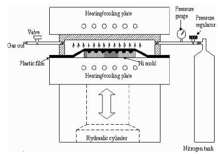
Fig. 1. Set-up of gas-assisted hot embossing
The pressure distribution is much more uniform over the whole contact area. Because the gas pressure is isotropic, no significant unbalanced forces are applied. The result shows promise for replicating microlens array on large plastic films with high uniformity.
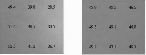
Fig. 2. (a) – Conventional hot embossing, (b) – Gas-assisted Imprinting. Pressure distribution in conventional hot embossing and gas-assisted hot embossing
Fig. 3 shows a SEM image of molded microlens and surface profile of a single microlens. The arrays of plastic microlens with diameter 150µm, pitch 200µm and height 36µm have been successfully replicated under the condition of 180°C, 40 kgf/cm2 and 90 seconds. The deviation of replicated microlens array released from the Ni mold is less than 0.25%. These results indicate good uniformity and controllability of the gas-assisted hot embossing for efficient fabrication of micron-scale structures.
3. Electromagnetic force-assisted imprint
Fig. 4 shows the electromagnetic force-assisted imprinting facility with UV exposure capacity used in the current experiment. The system consists of a UV-transparent top plate (glass plate), an imprinted substrate, an UV-lamp, and an electromagnet with power supply. The current of electromagnet is controlled by the power supply, thus the imprinting magnetic force is controlled. The UV intensity at 365nm is 100mJ/cm2 and the UV-curing dose is equal to the intensity of UV-light times the curing time. A UV curable resin is used.
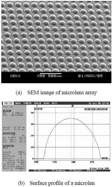
Fig. 3. SEM image and surface profile of molded microlens
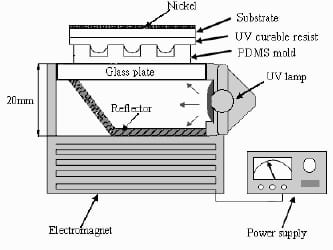
Fig. 4. Schematic diagram of electromagnetic force-assisted imprinting equipment
The experimental results are shown in Fig. 5. Under the condition of pressing for 30 seconds, UV curing for 0.5 minute and imprinting pressure of 1.6kgf/cm2, the sub-micron pattern with a line width of 500nm, a pitch of 1um and a feature height of 200nm can be successfully fabricated over the whole substrate. The average width of line is 502.4nm with a standard deviation of 2.8nm. The average height of lines is 197.9nm with a standard deviation of 5.8nm. In order to characterize the uniformity obtained from this process, the surface profile of 50 micro-lines from a single process run is measured and analyzed in Fig.6. These results indicate a good uniformity and controllability of the electromagnetic force-assisted imprinted submicron-scale structure.
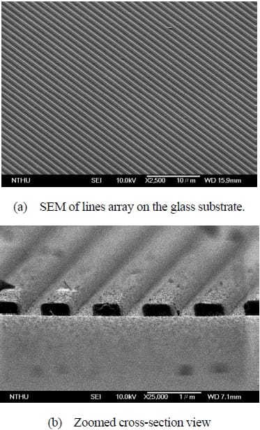
Fig. 5. SEM image of electromagnetic force-assisted imprint structures
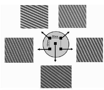
Fig. 6. SEM images of electromagnetic force-assisted imprint pattern at four corners and center on substrate
In order to reduce the imprinted pressure further and to expand the application of this method, the electromagnetic force assisted imprint system is modified. In this method, the ferromagnetic UV-curable resist is made of nano Fe powders mixed in UV-curable resist (the concentration in weight percentage is 4.8wt%). When the electromagnet is turned on, the magnetic UV-curable resist is pressed and attracted into the submicron scale structures of PDMS stamp. The liquid photopolymer is then cured by UV-irradiation at room temperature. Fig. 7 shows a SEM image of molded sub-micron scale pattern with a line width of 504nm, a pitch of 1.4um and a feature height of 203.5nm under the condition of pressing time of 30 seconds, UV curing time of 0.5 minute and imprinting pressure of 0.92kgf/cm2. This result indicates that using the ferromagnetic UV-curable resist can reduce the imprint pressure during the electromagnetic force-assisted imprint process, as shown in Fig. 8. It is also confirmed that the electromagnetic force-assisted imprinting process possesses great potential for producing sub-micron scale structures at room temperature and low pressure associated with good quality.
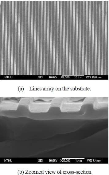
Fig. 7. SEM image of imprinted structures of ferromagnetic UV-curable resist
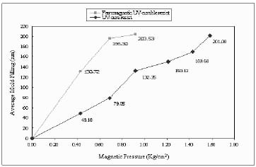
Fig. 8 Comparison of mold filling varying with magnetic pressure
4. Conclusions
In this study, three innovative methods of uniform imprint for micron and sub-micron features are presented. The corresponding novel facilities have been designed, constructed and tested. Under the proper processing conditions, the polymeric micron and sub-micron scale structure can be uniformly fabricated. Scanning electron microscopy (SEM) observations confirm that the imprinted structures are produced without defects and with good pattern fidelity over a large area. These imprint methods shown here appear as good alternative to the current mainstream imprint techniques. The high efficiency of the proposed fabrication process illustrates its potential as a direct and inexpensive route for various applications, especially in micron and sub-micron features.
Acknowledgements
This work was partially supported by the National Science Council of Taiwan under contract NSC94-2212-E007-004. The experimental work was conducted at Polymer Processing Laboratory of National Taiwan University.
References
- S.Y. Chou, P.R. Krauss, P.J. Renstrom, Nanoimprint lithography, Journal of Vacuum Science and Technology B 14 (1996) 4129-4133.
- S.Y. Chou, P. R. Krauss, W. Zhang, L. Guo, L. Zhuang, Sub-10 nm imprint lithography and applications, Journal of Vacuum Science and Technology B 15 (1997) 2897-2904.
- N.S. Ong, Y.H. Koh, Y.Q. Fu, Microlens array produced using hot embossing process, Microelectronic Engineering 60 (2002) 365-379.
- Y. Zhao, T. Cui, Fabrication of high-aspect-ratio polymer-based electrostatic comb drives using the hot embossing technique, Journal of Micromechanics and Microengineering 13 (2003) 430-435.
- K.B. Yoon, C.G. Choi, S.-P. Han, Fabrication of Multimode Polymeric Waveguides by Hot Embossing Lithography, Japanese Journal of Applied Physics 43 (2004) 3450-3451.
- T. Bailey, B. Smith, B.J. Choi, M. Colburn, M. Meissl, S.V. Sreenivasan, J.G. Ekerdt, C.G. Willsona, Step and flash imprint lithography, Defect analysis, Journal of Vacuum Science and Technology B 19 (2001) 2806-2810.
- B. Vratzov, A. Fuchs, M. Lemme, W. Henschel, H. Kurz, Large scale ultraviolet-based nanoimprint lithography, Journal of Vacuum Science and Technology B 21 (2003) 2760-2764.
- U. Plachetka, M. Bender, A. Fuchs, M. Otto, B. Vratzov, B. Vratzov,T. Gilnsner, F. Lindner, H. Kurz, W
afer scale patterning by soft UV-Nanoimprint Lithography, Microe-lectronic Engineering 73-74 (2004) 167-171. - Y. Xia, G. M. Whitesides, Soft Lithography, Annual Review of Materials Science 28 (1998) 153-184.
- H.D. Inerowicz, S. Howell, F.E. Regnier, R. Reifenberger, Multiprotein Immunoassay Arrays Fabricated by Microcontact Printing, Langmuir 18 (2002) 5263-5268.
- K.E. Paul, M. Prentiss, G.M. Whitesides, Patterning spherical surfaces at the two-hundred-nanometer scale using soft lithography, Advanced Functional Materials 13 (2003) 259-263.
- W.M. Choi, O.O. Park, The fabrication of submicron patterns on curved substrates using a polydimethylsiloxane film mould, Nanotechnology 15 (2004) 1767-1770.
- W.M. Choi, O.O. Park, A soft-imprint technique for submicron-scale patterns using a PDMS mold, Microelectronic Engineering 73-74 (2004) 178-183.
- B. Heidari, I. Maximov, and L. Montelius, Nanoimprint lithography at the 6 in. wafer scale, Journal of Vacuum Science and Technology B 18 (2000) 3557-3560.
- H. Hocheng, T.T. Wen, S.Y. Yang, Replication of microlens arrays by gas-assisted hot embossing, Materials and Manufacturing Processes V23 (2008).