

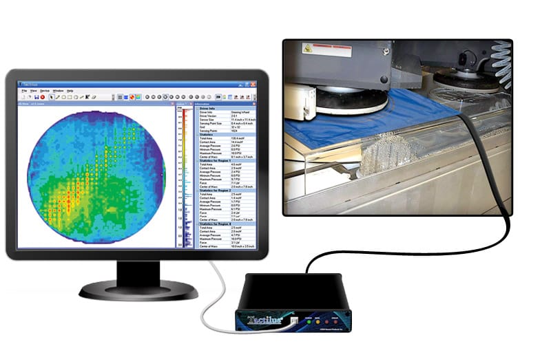

The Tactilus® wafer polishing system is designed to reveal parallelism and pressure uniformity problems between the polishing head and wafer component. Unlike conventional pressure transducers and load cells, Tactilus® is paper thin and is designed to be placed directly upon the active pressed surface ? yielding unprecedented visualization of your surface pressure profile.
Tactilus® Technology
Tactilus® is a matrix-based tactile surface sensor. Essentially an “electronic skin” that records and interprets pressure distribution and magnitude between any two contacting or mating surfaces and assimilates that data collected into a powerful Windows® based tool kit. Each Tactilus® sensor is carefully assembled to exacting tolerances and individually calibrated and serialized. The architectural philosophy of Tactilus® is modular allowing for portability, easy expansion, and simultaneous data collection of up to 4 discrete sensor pads. Tactilus® employs sophisticated mathematical algorithms that intelligently separate signal from noise, and advanced electronic shielding techniques to maximize the sensor?s resistance to noise, temperature and humidity.
“Our primary proposition is to offer the client precisely what they require or need. Everything we design with respect to the physical sensor element as well as our GUI and DLLs can be completely tailored to your unique situation.” – Jeffrey G. Stark, CEO
| Sensor Specifications | |
| Technology | Piezoresistive |
| Pressure Range | 0 – 142 PSI (0 – 10 kg/cm²) |
| Grid Size | 1 x 64 |
| Sensing Points | 64 |
| Sensor Dimensions | 0.4” x 32” (1 x 82 cm) |
| Scan Speed | 50 hertz |
| Spatial Resolution | 0.4” (9.35 mm) |
| Thickness | 36.8 mils (0.7 mm) |
| Accuracy | ± 10% |
| Repeatability | ± 98% |