

Article
Related Links
Yun-Biao Xin
Abstract
Pressure distribution at a wafer-pad contact surface in chemical-mechanical polishing has been modeled using finite element analysis. The model reveals the pressure abrupt increment at the wafer peripheral portion resulting from geometrical discontinuity at the contact edge. The amplitude of the pressure abruptness varies significantly with properties of polishing pad. Furthermore, the effect of pressurized retainer ring on the pressure distribution has been analyzed, illustrating the fundamental functions of the retainer ring in improvement of the wafer-pad contact pressure distribution.
1.Introduction
Chemical-mechanical polishing (CMP) has emerged as the most effective technology to achieve planarization to meet the challenge of shrinkage of design rule, and is expect to be used universally for all planarization steps starting from shallow trench isolation (STI) to top global interconnects in IC fabrication /1, 2, 3, 4/. With the explosive growth of CMP applications, in-depth understanding of fundamental mechanism that affects CMP non-uniformity becomes highly demanding. the pressure poses difficult challenging in realization of uniform distribution in a conventional rotational polishing system /9/.
Several attempts have been made to understand the pressure distribution at the wafer-pad interface under different contact modes in CMP as reviewed by Nanz /10/ and Komanduri /11/. Runnels /12/ conducted a tribological model by considering the shear stress arising from slurry flow, revealing the possibility of the fluid film between wafer and pad (hydroplaning) in CMP. The existence of the fluid film was recently confirmed by Coppeta’s novel experimental observation /13, 14/. Liu /15/ developed a model incorporating statistical methods into an elasticity theory and considering the contact of slurry particles with pad and wafer, indicating the dependence of removal rate upon the elastic moduli of slurry particle and polished film. Ticky /16/ recently worked on the interaction of wafer surface, pad asperity and Newtonian fluid film using 1-D Cartesian contact, predicting the variation of film thickness and fluid suction pressure with the applied pressure. However, when the contact is in a hydrodynamic condition where the wafer surface is supported by a film of slurry instead of polishing pad, recent experiments showed that the material removal was no appreciable /17, 18/ and independent of relative velocity /19/, and its removal rate did not follow Preston’s equation /18/. It indicates that the removal is primarily achieved by chemical action instead of prevailing mechanical abrasive action as seen in most CMP applications. Baker /20/ modeled pad-wafer as a solidsolid contact and treated the soft layer in a stacking pad as an elastic spring, elucidating the contribution of the pressure peak to edge roll-off. Wang /21/ solved the similar problem using finite element analysis and observed the similar results as Baker’s.
All of the documented work in solidsolid modeling is confined to the regime of wafer-pad interface exclusive of the contribution from retainer ring. The fundamental mechanism of retainer rings, albeit wide applications in CMP to prevent excessive removal at the wafer edge, has not been thoroughly explored. The purpose of the present work is to investigate the pressure distribution in wafer-pad contact surface in a mechanistic point of view. The pressure abrupt increment at the wafer periphery, responsible for non-uniform removal in CMP, is captured by the model and consistent with experimental observations. Furthermore, the model reveals the fundamental functions of retainer ring in improvement of the interface pressure distribution, thereby providing guidance for retainer-ring design and application.
2. Problem Formulation
In a conventional rotational mechanical-chemical polishing system as shown in Fig. 1, a wafer held by a backing film and retainer-ring in a rotational hub is pressed against a rotational polishing pad upon which slurry is dispensed. Polishing pressure is applied uniformly to the back side of the wafer via the hub, but the material removal is dictated by the waferpad contact pressure which varies on the wafer surface due to geometry discontinuity at the wafer periphery. The determination of the pressure profile at the contact surface is the focus of the analysis.
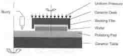
Figure 1: A rotational single-side polishing system.
For simplicity, the wafer-pad interface as shown in Fig. 2(a) is assumed to be full solid-solid contact with compliant displacement in axis r, regardless of the contribution of slurry hydrodynamic pressure, pad asperities, and contact-surface instability as analytically discussed by Galdwell /22/.

Figure 2: Schematic of wafer-pad interface modeling: a) without retainer ring and b) with retainer ring
Materials such as backing film, silicon wafer and retainer ring are considered to be isotropic and deformed in an elastic regime. The polishing pad is modeled as a composite material of different layers, with continuation of displacements (radius and axis) in the interfaces. The retainer ring as shown in Fig 2(b) is assume to be rigid with similar elastic constants as silicon. Wafer and pad deformations, axisymmetric with respect to geometry, loading and deformation, are governed by plate equations /23/ as:
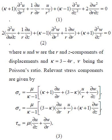
The associated boundary conditions are (1) Backing film top surface Applied pressure P0
Displacement. z = constant (z = h1 + h2 + h3 + h4 + h5, – R0 = r = R0)
(2) Fixed displacements at the bottom of pressure-sensitive adhesive (PSA) layer u = w = 0 (z = 0, – L ≤ r ≤ L) .
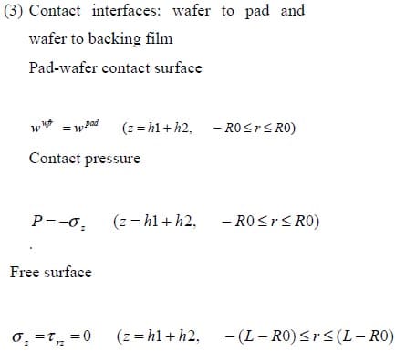
The contact pressure z S22 = -σ at the wafer-pad interface is solved by finite element analysis using ABAQUS 5.6 with 4 node-belinear reduced integration axisymmetric plate elements. Material properties used in the calculation, adopted from /20/ and /21/, are listed in Table 1.
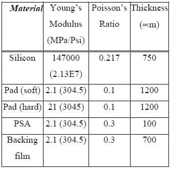
Table 1 Material Properties used in the modeling
3. R
esults and Discussion
In the following elastic analysis, normalization is adopted for generalization. The vertical axis represents the wafer-pad contact stresses normalized by the applied pressure P0, which is 5 (psi), and the horizontal axis stands for the distance from the wafer center normalized by wafer radius R0.
Stress components at the wafer contact surface are depicted in Figure 3. S11, S12 and S22 are stresses at r, r-z and z directions, respectively. The pressure (- normal stress S22) on the wafer surface can be divided into three regions. The first is the plateau region at the wafer interior, where pressure is uniformly distributed. The second is the abrupt region at the wafer periphery where pressure has a sudden increment resulting from the geometry discontinuity at the edge of wafer-pad contact. The Third is the transition region between the 1st and 2nd regions where the pressure is slightly lower than the applied pressure. These three pressure regions give rise to three corresponding removal zones in CMP – uniform, fast and slow, in that the removal rate is controlled by the contact pressure /5, 6, 7/. The pressure profile on the surface matches well the remnant oxide thickness after CMP /24, 25, 26/, indicating that the formation of excessive removal at the wafer peripheral portion (so-called edge roll-off) is attributed from the pressure abrupt increment at the wafer periphery.
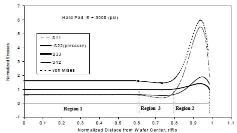
Figure 3: Stress distributions on the wafer surface in the interface.
Von Mises stress follows the similar profile as pressure distribution as shown in Fig. 3, which agrees with Wang’s modeling result /21/. Wang /21/ used Von Mises stress to describe the removal non-uniformly at the wafer edge, emphasizing on the fact that removal was realized by plastic shear deformation. In chemical-mechanical polishing, the materials removal is primarily achieved by brittle indentation /6,7/. Furthermore, all of the experiments have shown that the removal rate is governed by the applied pressure /5, 7/. Therefore, the contact pressure on the wafer surface, signifying the physics of the material removal mechanism, is used to in the analysis.
3.1 Effect of Polishing Pad on Contact Pressure Distribution
Properties of polishing pads, such as thickness, porosity, hardness, and stacking, are studied individually to reveal its impact on wafer-pad pressure distribution. The effect of pad hardness on the pressure distribution is depicted in Fig. 4. The pad hardness has a profound impact on the pressure distribution.
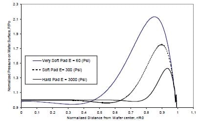
Figure 4: Effect of pad hardness on the pressure distribution.
Both the amplitude of the pressure peak and the width of non-uniform pressure regions at the wafer edge increase with the decreases with pad hardness. The pressure abruptness at the wafer peripheral portion comes from the deformation discontinuity at the contact periphery. Hard pads with less deformation alleviate the disparity, which reduces the pressure abruptness and achieve better uniformity with less edge roll-off in CMP. The result is not only consistent with the experiment /27/ that hard pads improved both within-wafer and within-die nonuniformity, but also in good accordance with our experimental observation as shown in Fig. 5. In the experiment, a pressuresensitive Pressurex-Micro film with a carbon-based layer (manufactured by SPI Sensor Products) was placed between a pad and a 4” polished silicon wafer to qualitatively characterize the interface pressure distribution. The gray level in the film correlates with the pressure amplitude. Figure 5 shows that there exists a deep dark region at the wafer periphery in a soft rubber pad, indicating a sudden pressure increment at the edge. But this kind of the region was not observed in a hard H-2 pad made by Rodel (pressure increment is lower than the film sensitivity), indicative of lower pressure increment at the periphery in the hard pad.
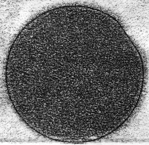
Figure 5: Images of Pressurex-micro film under the applied pressure of 3 (psi): rubber pad
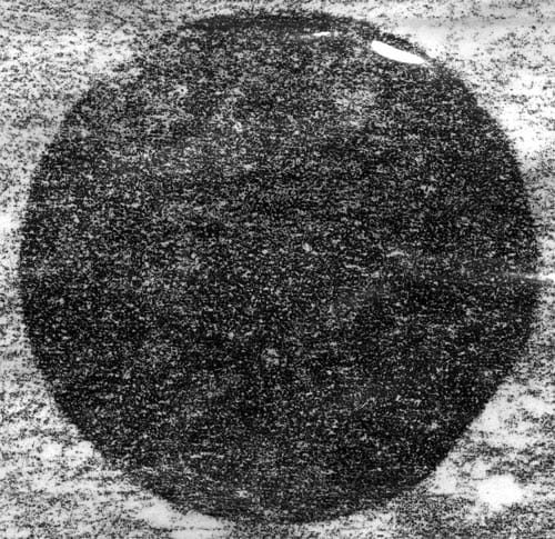
Figure 5: Images of Pressurex-micro film under the applied pressure of 3 (psi): Rodel H-2 pad.
The effect of pad thickness on the pressure distribution is illustrated in Fig. 6. The amplitude of the pressure peak at the wafer edge enhances with the increases of pad thickness, suggesting that a thinner pad improves CMP non-uniformity due to less deformation, which agrees with Baker observation /20/. It is noticed that contact stiffness increases with the reduction of pad thickness, which might induce some adverse effect (such as wafer breakage) in CMP.
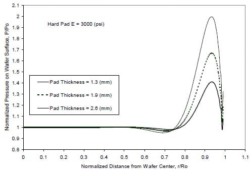
Figure 6: Effect of pad thickness on the pressure distribution.
Most pads used in CMP processes are porosity-natured to facilitate slurry transportation. The effect of pad porosity is simulated by the variation of its Poisson Ratio. High porosity yields low Poisson ratio due to low polymer content. Figure 7 suggests that the contribution of the porosity to the pressure distribution is negligible. Stacking pads have bee popularly used in CMP applications with the merits of both soft and hard pads.
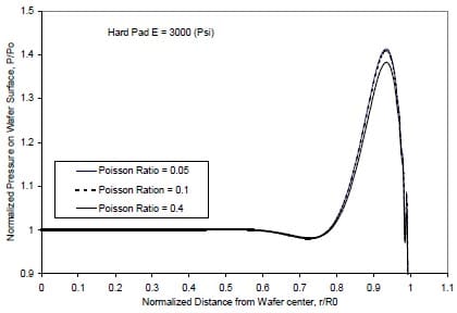
Figure 7: Effect of pad porosity on the pressure distribution.
Usually, a hard pad (such as Rodel IC1000) lays on the top of a soft pad (such as Rodel Suba IV). The top hard pad provides a stiff plane for achieving better local planarization. The bottom soft pad offers a cushion to the contact surface and conformability to wafer topology so as to achieve better within-wafer uniformity. The effect of stacking pad on the pressure distribution is shown in Fig. 8.
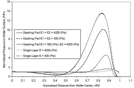
Figure 8: Effect of stacking pad on the pressure distribution.
The thickness of the stacking pad is twice of the single-layer pad. For the same pad hardness, the amplitude of the pressure abruptness at the wafer edge in the doublelayer stacking pad is much higher than the one in the single-layer pad due to the increase of pad thickness as discussed above. The behavior of stacking pad goes between soft and hard stacking pads at the same thickness, but possesses a high pressure abruptness in comparison with the single-layer, because the pad thickness has a more predominant effect on the pressure distribution than the hardness does. The profile of the pressure distribution in the stacking pad is qualitatively in accordance with Baker’s model and experiments /20/.
3.2 Effect of Retaining Ring on Contact Pressure Distribution
The pressure abruptness at the wafer edge is attributed from the geometrical discontinuity at the wafer-pad contact periphery. The most effective approach to lessen the edge effect is to either move the abrupt region away from the wafer surface, or to alleviate the discontinuity. The function of a pressurized retainer ring as shown in Fig. 2 (b) is analyzed as follows:
Figure 9(a) depicts the effect of retainer-ring pressure on the pressure distribution. The amplitude of the pressure peak reduces with the increase of the retainer-ring pressure, suggesting that the pressure applied on the retainer-ring should be lar
ger than the pressure applied on the back surface of the wafer to achieve a desirable result, in that the pad rebounding at the wafer edge is suppressed effectively as shown in Fig. 9(b). This result is consistent with the claims in the patents applied by CMP system suppliers: Applied Materials, Inc. /28, 29/, Cybeq Systems, Inc. /30/, Ebara Corp. /31/, and Integrated Process Equipment /32/.
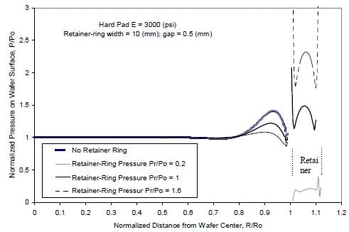
Figure 9: Effect of retainer ring on the pressure distribution and displacement: pressure distribution
There are two important geometrical components in the retainer ring: retainerring width and inner diameter. The former determines the contact area; the latter controls the gap between the wafer periphery and retainer-ring inner diameter.
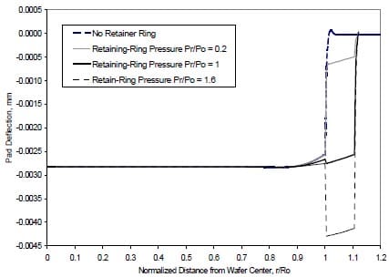
Figure 9: Effect of retainer ring on the pressure distribution and displacement: pad displacement.
The effect of the width on the contact pressure distribution is shown in Fig. 10. In the range considered in the calculation, the retainer-ring width does not have a noticeable effect on the pressure distribution.
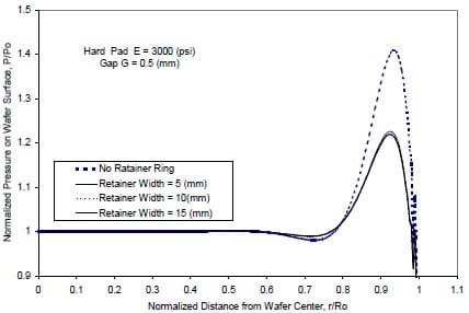
Figure 10: Effect of retainer-ring width on the pressure distribution.
Figure 11 reveals the effect of the retainerring gap on the pressure distribution.
The retainer-ring gap has a significant impact on the pressure distribution. The amplitude of the pressure peak at the wafer edge decreases with the reduction of the gap. The effectiveness of the retainer ring diminishes with the increase of the gap. The analysis reveals two fundamental functions of the pressurized retainer ring in preventing peripheral portion of the wafer from being polished excessively, besides holding the wafer in place during polishing. One is to virtually extend wafer contact surface so as to shift the pressure abruptness away from the wafer useful surface as shown in Fig. 11; the other is to suppress pad rebounding at the wafer edge to alleviate the extent of geometrical discontinuity. For effectiveness of retainer rings, pressure on the retainer ring should be slightly higher the surface pressure and the gap between the wafer periphery and retainer-ring inner diameter should be minimal.
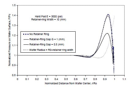
Figure 11: Effect of retainer-ring gap on the pressure distribution
4. Concluding Remarks
In the communication, we have modeled the wafer-pad contact pressure distribution using finite element analysis. Interfaces between wafer and polishing pad, and retainer-ring and polishing pad are treated to be contact surfaces to simulate the nature of polishing process.
The model predicts the existence of pressure abruptness at the peripheral portion, which is attributed mainly to geometry discontinuity at the wafer-pad contact edge. Polishing pads have a significant impact on the pressure distribution. Less pad deformation can reduce the pressure abruptness and improve the uniformity in CMP. The amplitude of the pressure peak at the wafer edge increases with the decrease of pad hardness, which is consistent with experiment observations. The abrupt increment of the contact pressure at the wafer edge, giving rise to excessive material removal at the wafer peripheral portion, is one of the root causes for the formation of edge roll-off in CMP. In addition, the effects of pad properties such as thickness, porosity and stacking on the pressure distribution have been revealed.
Furthermore, an important contribution made by the present study is that the model reveals the fundamental functions of retainer ring. With an independent pressure applying upon the retaining ring, the retaining ring can not only suppress the pad rebounding at the wafer periphery, but also extend the virtual contact surface as so to improve the pressure distribution significantly at the wafer peripheral portion. The model indicates that the gap between the wafer periphery and retainer-ring inner diameter has a profound impact on the effectiveness of retainer rings.
To make the problem tractable, the model developed here is deliberated simple. Many approximations are made. The materials considered are assumed to be elastic and isotropic. The model assumes that the interface between wafer and polishing pad is a solid-solid contact, and ignores hydrodynamics at the wafer edge and slurry distribution. The quantitative features of the pressure distribution such as the exact amplitude of pressure increment at the wafer periphery may be compromised by the approximations in the model. Nevertheless, the essential qualitative physics of the pressure distribution at the wafer-pad contact surface is captured, revealing the root source of the edge roll-off and fundamental functions of retainer rings in CMP.
Acknowledgements
The author is grateful to Dr. G. Xu in Ford Motor for helpful discussion, and Dr. L. Xia in Hibbitt, Karlson and Sorensin, Inc. for assisting the program debugs and bringing contact elements to my attention. The author would like to thank Mr. J. Jose for assisting an experiment, Dr. H. Erk for supporting the work and MEMC for approving the publication.
References
- Ali, I, Roy, SR and Shinn, G. Chemicalmechanical polishing of interlayer dielectric: a review. Solid State Technology 1994;10: 63-70.
- Sethuraman, AR. CMP – past, present and future. Future Fab International 1998:261-264
- DeJulie, R. CMP grows in sophistication. Semiconductor International 1998; 11: 56-80.
- Singh, R, Parihar, V and Poole, KF. Semiconductor manufacturing in the 21st century. Semiconductor Fabtech 1999; 9: 223-232.
- Preston, FW. The theory and design of plate glass polishing machines. J Soc Glass Tech 1927; 11: 214-257.
- Cook, L. Chemical processes in glass polishing. J Non-Crystalline Solids 1990; 120: 152.
- Tseng, W-T and Wang, Y-L. Reexamination of pressure and speed dependencies of removal rate during chemical-mechanical polishing processes. J Electrochem Soc 1997;144:L15-L17.
- Zhao, B and Shi, F. Chemical mechanical polishing in IC process: new fundamental insights. Proceedings of 4th International Chemical-Mechanical Planarization for ULSI Multilever Interconnection Conf (CMP-MIC), Santa Clara, CA: 1999;13-21.
- Hansen DA, Sun, H and Wall, R. Linear velocity and its effect on planarity. Proceedings of 4th International Chemical-Mechanical Planarization for ULSI Multilever Interconnection Conf (CMP-MIC), Santa Clara, CA: 1999; 417-420.
- Nanz, G and Camilletti, L. Modeling of chemical-mechanical polishing: a review. IEEE Transactions on Semiconductor Manufacturing 1995; 8(4): 382-389.
- Komanduri, R, Lucaa, DA. and Tani. Y. Technological advances in fine abrasive processes. Annals of the CIRP 1997; 46: 545-596.
- Runnels, SR and Eyman, LM. Tribology analysis of chemical-mechanical polishing. J Electrochem Soc 1994; 141(6):1698-1701.
- Coppeta, J, Rogers, C, Philipossian, A, Kaufman, FB. Characterizing slurry flow during CMP using laser induced fluorescence. Proceedings of the 2nd International Chemical-Mechanical Polish for ULSI Multilevel Interconnection Conference, Santa Clara, CA: 1997.
- Coppeta, J. Rogers, C, Racz, L etc. The influence of CMP process parameters on slurry transport. Proceedings of 4th International Chemical-Mechanical Planarization for ULSI Multilever Interconnection Conf. (CMP-MIC), Santa Clara, CA: 1999:37-44.
- Liu, C-
W, Dai, B-T, Tseng, W-T, and Yeh, C-F. Modeling of the wear mechanism during chemicalmechanical polishing. J Electrochem Soc 1996; 143(2): 716-721. - Ticky, J, Lever, J, Shan, L and Danyluk S. Contact mechanics and lubrication hydrodynamics of chemical mechanical polishing. J Electronchem Soc 1999; 146(4): 1523-5128.
- Levert, JA, Mess, FM, Richard, F, etc. Mechanisms of chemical-mechanical polishing of 2 SiO dielectric on integrated circuits. Tribology Transactions 1998; 41(4): P593-599.
- Bhushan, M, Rouse, R and Lukens, JE. Chemical-mechanical polishing in semidirect contact mode. J Electrochem Soc 1995; 142(11): 3845-3851.
- Thornton, B, Nagengast, A, Pallinti, J, etc. High speed polishing of silicon dioxided thin films using linear planarization technology. Proceedings of the 2nd International Symposium on Chemical Mechanical Planarization in Integrated Circuit Device Manufacturing, the electrochemical society: 1998; 90-96.
- Baker, AR. The origin of the edge effect in chemical mechanical planarization. J Electrochem Soc 1996 ECS Fall meeting, San Antonio, TX: 1996; 1-7.
- Wang, D, Lee, J, Holland, K, etc. von Mises stress in chemical-mechanical polishing processes. J Electrochem Soc 1997; 144(3): 1121-1127.
- Gladwell, GM. Unbonded contact between a circular plate and an elastic foundation. Proceedings of the Symposium of the International Union of Theoretical and Applied Mechanics (IUTAM), Enschede, Netherlands: 1974; 99-109.
- Gecit, M. Axisymmtric contact problem for a semi-infinite cylinder and a half space. Int J Eng Sci 1986; 24(8): 1245- 1256.
- Tanaka, K, Hashimoto, H and Suzuki, F. Polishing member and wafer polishing apparatus. Shin-Etsu Handotai, Japan, US Patent No. 5,564,965: 1994.
- Breivogel, J, Prince, M and Barns, C. Method and apparatus for chemical mechanical polishing using pneumatic pressure applied to the backside of a substrate. Intel, Corp, US Patent No. 5,635,083: 1995.
- Chen, HC, Chen, CH, Wei, YT, Wu, JY and Lur, W. Global planarized CMP using conditioning technology. Proceeding of 4th International CMP for ULSI Multilevel Interconnection Conference (CMP-MIC) 1999.
- Philipossian, A. Tutorial on chemical mechanical polishing (CMP). Intel Corp, Santa Clara, CA, USA, Rev. 1, Sept. 1999
- Shamouilian, S and Shedon, N. Carrier head with a layer of conformable material for a chemical mechanical polishing system. Applied Materials, Inc., US patent No. 58204448: 1996.
- Guthrie, W and Cheng, T. Method and apparatus for using a retaining ring to control the edge effect. Applied Materials, Inc., US Patent No. 5,795,215: 1996.
- Shendon, N, Struven, K and Kolenkow, R. Wafer polisher head having floating retainer ring. Cybeq System, Inc., US Patent No. 5,205,082: 1991.
- Kimura, N and Yasuda, H. Polishing apparatus. Ebara Corp., European Patent No. 0870576-A2: 1998.
- Jackson, P and Schultz, S. Pneumatic polishing head for CMP apparatus. Integrated Process Equipment Corp., US Patent No. 5,643,061: 1995.
![]()