Surface Profiling is the process of quantifying the roughness of a surface. The device used to perform surface profiling is called a profilometer. There are two general types of profilometers: contact and non-contact. Vertical resolution is usually in the nanometer level although lateral resolution is poorer.
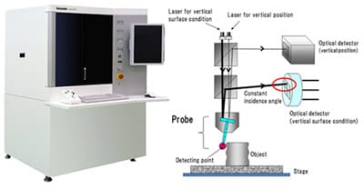
Contact profilometers use a diamond stylus that touches the surface to be profiled. The radius of the stylus ranges from 20 nm to 25µm, and the stylus tracking force is less than 50 mg. As the stylus moves against a surface, its displacement is converted into a digital signal that is stored, analyzed, and displayed by the profilometer. Most of the world’s surface finish standards are written for contact profilometers. In addition, contacting the surface is often an advantage in dirty environments. Figure 1 is a picture and operational schematic of the Panasonic 3D profilometer.

Fig 1: 3D Profilometer by Panasonic
Non-contact, or optical, profilometers are also used for surface profiling. Optical profilometers use various techniques for profiling, such as: laser triangulation, confocal microscopy, and digital holography. Non-contact profilometers are reliable and very fast. The optical spot size is in the micrometer range.
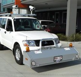
Surface profiling of roads is a popular application for non-contact profilometers. This involves the identification, measurement, and recording of pavement road-surface defects. As shown in Figure 2, small vans are fitted with laser profilometers to perform digital imaging surveys. As the van is driven along the road, the profilometer collects data that document the roughness, rutting, and surface texture of the roadway. These data are used for verification of deterioration rates as well as the basis for planning maintenance.

Fig 2: Van Fitted with a Laser Profilometer.
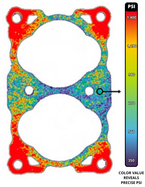
Another method for performing surface profiling is the use of Fujifilm Prescale®, pressure indicating sensor film, which has been used effectively in the surface profiling of wafers being polished. Fujifilm Prescale® is a Mylar®-based film that contains a layer of tiny microcapsules. The application of force upon the film causes the microcapsules to rupture, producing an instantaneous and permanent high-resolution “topographical” image of pressure variation across the contact area.
Simply place Fujifilm Prescale® between any two surfaces that touch, mate, or impact, such as the grinding head and the wafer. Then, apply pressure and remove it. Immediately, the film reveals the distribution of surface force pressure between the two surfaces. Conceptually similar to Litmus paper, the color intensity of Fujifilm Prescale® is directly proportional to the amount of pressure applied to it. Since the grinding head is very flat and highly polished, the pressure distribution is equivalent to the surface profile where high pressure indicates a raised area on the wafer.
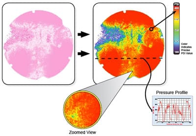
The left-most picture in Figure 3 shows the Fujifilm Prescale® image of surface pressure against the wafer. The darker areas indicate the elevated regions of the wafer, and the white areas indicate the lower elevations. Further processing of this image (as shown at the right of Figure 3) provides enhanced digital visuals and statistical data.

Fig 3: Fujifilm Prescale® Used for Surface Profiling of a Wafer during Polishing


