Sung-Won YOUN*, Hiroshi GOTO, Shoji OYAMA1, Masaharu TAKAHASHI, and Ryutaro MAEDA
Advanced Manufacturing Research Institute (AMRI), National Institute of Advanced Industrial Science and Technology (AIST),
1-2-1 Namiki, Tsukuba, Ibaraki 305-8564, Japan
1Design Engineering Group, Engineering Department, Hirose Sensing Technology (HST) Co., Ltd.,
Kaneko No. 2 Building 8F, 2-6-23 Shinyokohama, Kohoku-ku, Yokohama 222-0033, Japan
Abstract
The study aims to investigate the possible defects that may occur during imprinting of poly(chloro-p-xylylene) (parylene-C) film (thermal oxidation, delamination, thermal cracking and insufficient filling at the periphery) and to overcome them by modifying the process conditions and mold design. X-ray diffraction (XRD) analyses results for the parylene-C films indicated that higher deposition pressure leads to a lower crystallinity of parylene-C film. By tuning the process conditions and mold design, patterned fields (composed of arrays of 25-mm-high, 10-mm-wide and 1-mm-long lines with 10 mm spacing) in 0.4- mm-thick and 20-mm-sized nickel molds could be successfully replicated on 60-mm-thick parylene-C films deposited at both 25 and 45 mTorr. Complete filling over the whole imprint area could be achieved at < 270 °C with the press force at 2 kN and the press hold time of 900 s with the aid of an implemented dummy pattern. Both thermal cracking and delamination could be avoided, even at 270 °C, under the established process conditions and mold design with the help of an adhesion promotion treatment of silicon substrates (SF6 plasma etching for 2 min and spin-coating of KBM-503-based solution). Furthermore, the molds used for paryelne imprinting could be cleaned by dipping in chloronaphthalene solution at >175 °C, followed by an oxygen plasma etching.
Keywords: imprint lithography, thermal imprint, parylene-C, micromold
Introduction
Poly(chloro-p-xylylene) (parylene-C), which is a thermoplastic/ linear-crystalline polymer, is being widely applied to bio- and optical microdevices because of its favorable properties such as stress-free conformal deposition, high mechanical flexibility, low defect density, chemical inertness, biocompatibility, optical transparency and very low thermal conductivity.1–6) Furthermore, parylene is compatible with traditional microfabrication technology and is suitable for multilayer processing to fabricate complex structures. In the recent few years, numerous parylene-based microdevices (microvalves, DNA separation/detection channels, gas chromatographic column, shear stress sensors, and microspeakers) have been fabricated by various methods such as direct parylene deposition with/without a sacrificial layer,2) dry etching [plasma, reactive ion etching (RIE), and deep reactive ion etching (DRIE)]4) and micromolding.5,6)
The imprint process of thermoplastic polymers is a mature process, but it is gaining renewed attention as a good candidate for high-volume production of microdevices.7–12) The ability of the conformal deposition of parylene is one of the crucial merits for imprinting because it enables the formation of stress-free thin films (with well-controlled thickness) on all exposed surfaces, and absolute even layer formation even on corners. The film thickness is one of the main factors that strongly affect the flow rate of material during embossing.13,14) However, to our knowledge, imprint technologies have not been used for microstructuring parylene since this material has several drawbacks as an imprint material, such as a high melting temperature, high molecular weight (Wt, 500,000) and high crystallinity.15) Generally, a high-molecular-weight polymer has a large shear modulus, making it relatively hard to deform above the glass transition temperature (Tg).16,17) Additionally, the heating of parylene can cause the hardness to increase as the result of density and crystallinity increases.15) Thus, particularly for an imprinting parylene, the subtle tuning of process parameters (temperature, pressure and time) and the fabrication of a well-designed mold are crucial.
It is known that, in general, a good replication result can be achieved when the imprint temperature is set higher than the flow temperature (Tf) of the polymer, because the modulus and viscosity are markedly reduced above Tf. In the viscous-liquid flow-state regime (>Tf), the motion of entire chains takes place and the polymer flows by chain sliding, rendering the deformation irreversible, which makes it the suitable temperature range for patterning.8) It has also been reported that an optimal imprinting temperature is generally found 70 – 80 °C above the Tg of the material used.8) In contrast, to imprint parylene-C, the imprinting temperature must be set much higher than that of general emboss materials because the Tf of parylene-C is about 230 °C (Tg þ 140 °C), as known the modulus-temperature curves in the literature.18)
In this study, the possible defects (thermal oxidation, delamination, thermal cracking and insufficient filling) that may occur during parylene-C imprinting were investigated and overcome by modifying the process conditions and mold design. To accomplish this, a series of experiments were performed. First, four different types of positive-tone nickel molds (in terms of thickness, size and patterned field geometry) were prepared by a silicon micromachining process, followed by electroplating. Then, a series of imprint tests were performed under various process conditions (temperature: 200, 230, 250, 260, 270 °C; force: 200 kgf; press-hold time: 300, 2000, 2400, 1800 s, unloading conditions during cooling) using the fabricated molds and parylene-C films (deposited at 25 and 45 mTorr). Prior to imprint tests, the differences in the crystallinity among parylene-C films deposited at different pressures were analyzed by an X-ray diffraction (XRD) method, and the relationship between the thickness of parylene-C film and the amount of dimer was measured. Finally, the cleaning of molds was attempted using both chloronaphthalene solution and oxygen plasma.
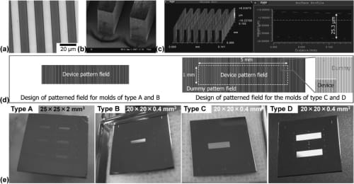
Fig. 1. Nickel molds used for thermal imprint tests. (a) Optical, (b) SEM, and (c) optical interferometric images of microstructures in patterned fields. (d) Scheme of designs for patterned fields and (e) photographs of the fabricated molds.
2. Experimental Procedure
2.1 Preparation of Parylene-C film
Parylene-C was chosen as the imprint material (glass transition temperature, Tg: 90°C; melting point, Tm: 290 °C). Parylene-C/silicon samples were prepared
by vapor deposition polymerization using a PDS2010 Labcoater (Specialty Coating Systems, U.S.A.) according to the following deposition process. The first step was the vaporization of the solid di(para-xylylene) dimer (white crystalline powder, DiX-C, Daisankasei, Japan), which was loaded in the vaporizer of the machine, at 110 –150 °C. The second step was the pyrolysis of the dimer at about 680 °C while passing the vapor through the furnace to yield the stable monomeric diradical, para-xylylene. Lastly, the monomer reached the room-temperature deposition chamber where it simultaneously adsorbed and polymerized evenly on Si substrates. Prior to parylene-C deposition, Si wafers were etched using a SF6 plasma for 2 min and then spin-coated with an adhesion promoter (KBM-503-based solution on Si wafers). Parylene-C films were deposited at the pressures of 25, 35, 45, and 55 mTorr. Parylene-C/silicon samples were then cut to 25 x 25mm2 (for the type A mold, refer Fig. 1) and 15 x 15mm2 (for the type B, C, and D molds) in size by dicing.
2.2 Nickel mold fabrication
Four different types of positive-tone nickel molds (types A, B, C, and D) of different sizes (25 x 25mm2 for type A and 20 x 20mm2 for types B, C, and D) and thickness (2mm for type A and 0.4mm for types B, C, and D) were prepared by a silicon micromachining process such as DRIE, followed by an electroplating (Fig. 1). The patterned fields in all molds were composed of arrays of 25-mmhigh 10-mm-wide, and 1 mm-long lines with 10 mm spacing [Figs. 1(a)–1(c)], but had two different geometries [Fig. 1(d)]. All molds had patterned fields over their customized partial area, as shown in Fig. 1(e).
2.3 Thermal imprint tests
Thermal imprint tests were conducted using hot-pressing equipment (maximum applied force: 2 kN; maximum heating temperature: 700 °C; vacuum pressure: <1 pa) with an imprint velocity at 0.05mmmin and heating rate of 0.5 °cs. since positive-tone molds were used in this study, the placed on bottom press-head to avoid mold deformation.19) first step process, was pressed into a parylene-c film preset temperature (well above tg of parylene-C). The pressing force and temperature were then held for a sufficient time to achieve complete filling. After cooling to 80 °C (below Tg) the applied force was released and the nickel mold was removed from the parylene-C sample. The uniformity of imprint force across the whole imprint area was evaluated using a pressure-sensitive film (Prescale film, FUJIFILM, Japan), and compensated by using various types of spacers. GC-1720 (Sumitomo 3M, Japan) was used as the mold release agent.
2.4 Measurement
The thickness of parylene-C films was measured using a microfigure measuring instrument (Surfcorder ET4000M, Kosaka Laboratory, Japan). XRD analysis was performed for the structural characterization of the fabricated parylene- C films in a diffractometer using conventional θ=2θ geometry. Processed sample surfaces were observed by optical microscopy (OM) and a scanning electron microscope (SEM) and their morphological data, such as the structure dimensions, were measured using an interferometric surface profiler (Zygo New View 5000). Some imprinted parylene-C samples were overcoated with a thin metal layer of 25/100-nm-thick Ta/Cu to prevent charge-up during SEM observation.

Fig. 2. (a) XRD patterns (under θ=2θ scan geometry) of parylene-C at different deposition pressures. (b) Relationship between the thickness of parylene-C film and the amount of dimer. (c) Effect of deposition pressure on achieved film thickness with the same dimer amount.
3. Results and Discussion
Figure 2(a) shows the XRD data of parylene-C film deposited on Si substrates at different pressures of 25, 35, 45, and 55 mTorr. The obtained data showed that all samples have the same peak at 2θ equal to about 15°. Our data also indicate that the crystallinity decreased under deposition pressures above 45 mTorr. In general, a lower XRD peak intensity is generally obtained because of paracrystallinity or disorder in the crystalline unit cell. Thus, pinhole-free parylene-C film with a thicknesses of about 60 mm was conformally deposited at pressures of 25 and 45 mTorr for imprint tests (unless otherwise indicated, parylene-C samples deposited at 25 mTorr were used). The film thickness was tuned by varying the quantity of dimer. The thickness of the parylene-C film was set to be more than twice of the master structure height (of mold) to achieve easy relaxation of localized strain for easy material flow. The relationship between the parylene-C thickness and the amount of dimer is shown in Fig. 2(b). Higher deposition pressure allowed for shorter deposition time (16 h for 25 mTorr and 8 h for 45 mTorr), but caused material loss, as shown in Fig. 2(c). Previously, the parylene-C surface was cleaned by aircleaning and subsequently coated with a solution of a mold release agent. No other chemicals, such as acetone, were used for surface cleaning because they can attack parylene- C/silicon interfaces, resulted in the partial delamination of the parylene-C film.3)
There are several issues to be considered in order to achieve successful thermal imprinting of parylene-C. Here, some of them will be pointed out referring to typical imprint test results obtained using the mold of type A (Fig. 3). The first issue is the oxidative degradation of parylene-C, which can occur above 120 °C in air.20) In Fig. 3(a), the optical micrographs of typical samples imprinted in air are shown as examples. This defect did not occur in the thermal imprint tests in vacuum. A vacuum environment is also effective for avoiding air entrapment and nickel mold corrosion during thermal imprinting. Other issues are the delamination and thermal cracking of parylene-C film. As mentioned in the introduction, parylene-C itself has a high thermal expansion coefficient and high molecular weight. The results of imprint tests using the mold of type A showed that parylene-C is very difficult to deform even at 200 °C (¼ Tg þ 110 °C) because of its high molecular weight [Fig. 4(a)]. Under the imprint temperature of 200 °C, complete filling over an entire surface area could not be obtained even at 5 kN (in this case, another imprint system was used). In addition, the repetitive use of this pressure condition resulted in the deformation of the Ni master structures. Although the temperature was a more dominant factor than the pressure and time and complete filling could be achieved at 260 °C, replication uniformity over the whole pattern area must still be improved, particularly at the periphery [Fig. 4(b)]. Moreover, the imprint temperature condition above 200 °C could resulted in the cracking and delamination of a parylene-C film after cooling due to the large difference in the coefficient of thermal expansion (CTE) between silicon and parylene-C, as shown in Figs. 3(b) and 3(c). Such delamination occurred despite adhesion promotion treatment. By controlling the temperature profile during the cooling step and reducing the hold time at the maximum heating temperature, cracking was eliminated whereas the delamination problem was not fully solved. If there is no limitation in the type of substrate material, the use of another substrate material that has a more similar CTE to parlene-C may be another solution. The insufficiently compensated unevenness of the mold could be a possible reason for insufficient filling, delamination, thermal cracking and mold deformation (warping and distortion) because it could hinder the conformal contact with the sample surface, resulting in the nonuniform distributions of stress and temperature.21,22) Thus, the modification of the mold and process design was attempted.
3.1 Modification of mold and process design
First, a smaller and thinner mold (type B, refer Fig. 1) was designed and made. This mold is 20 x 20mm2 in size and has half the thickness of the type A mold. A thinner mold generally offers better conformal contact with a sample surface and reduces the pressure needed for complete filling during the imprinting step since it is more flexible (or deformable) than a thicker mold.8) Furthermore, only one patterned field at the center of the mold was designed to minimize the effect of mold unevenness. Figure 5(a) shows the scheme of the filling sequence in the patterned field observed in this study. Figures 5(b) and 5(c) show the imprinted patterns on the parylene-C surface under incomplete filling conditions. In order to get an overview of the patterned field, optical micrographs at various magnifications were taken. The filling of the patterned field started from the field’s central region and gradually expanded to the periphery. As shown in the low-magnification micrograph [Fig. 5(b)], a completely filled patterned region is brighter than an insufficiently filled region since it reflects more light upward due to the flatter top surface. As compared with an imprinted patterned field using the mold of type A (Fig. 4), the pile-up pads generated by squeeze flow of the material showed more uniform width along the periphery since the thinner and smaller mold provided better conformal contact with the sample surface, resulting in the decrease of the stress gradient and the local flatness distortion.
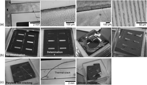
Fig. 3. Typical samples showing various defects that can occur during thermal imprinting. (a) Optical images of replicated parylene-C features by thermal imprinting in air (T ¼ 260 °C; P ¼ 200 kgf;tH¼ 300 s, where T, P, andtHare the temperature of top and bottom press-heads, pressing force, and press hold time, respectively. (b) Photographs of imprinted parylene-C/Si samples showing delamination of parylene film (T ¼ 200, 230, 250, 260 °C; P ¼ 200 kgf;tH¼ 2000 s). (c) Photograph and optical micrographs of parylene-C/Si sample showing both delamination and cracking (T ¼ 260 °C; P ¼ 200 kgf;tH¼ 300, 2000 s).

Fig. 4. Optical micrographs of patterns on parylene- C surfaces imprinted using type A mold under incomplete filling conditions: (a) T ¼ 200 °C; P ¼ 200 kgf; tH ¼ 2400 s and (b) Tmax ¼ 260 °C; P ¼ 200 kgf; tH ¼ 1800 s.
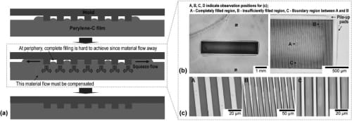
Fig. 5. (a) Scheme of filling sequence of parylene-C. (b, c) Optical images of the pattern on parylene surface imprinted using type B mold under incomplete filling conditions (T ¼ 250 °C; P ¼ 200 kgf; tH ¼ 900 s).
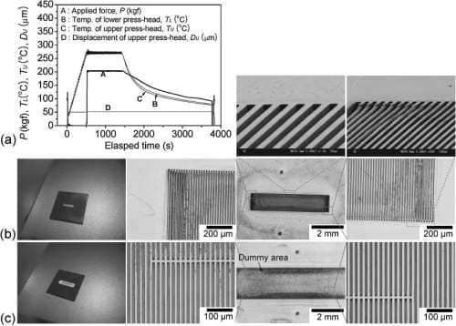
Fig. 6. Effect of dummy pattern on formability. (a) History of adopted conditions used in imprint tests (T ¼ 260 °C; P ¼ 200 kgf; tH ¼ 900 s). Photograph, and optical and SEM images of parylene-C surfaces imprinted using molds of (b) type B and (c) type C under the same imprint conditions.

Fig. 7. Filling characteristics at the interface between the device pattern field and the dummy pattern field. (a) SEM image showing observation position. (b–e) Patterns replicated at different temperatures.
To investigate the effect of the dummy pattern on formability, imprint tests were performed using the type B and C molds at 260 °C with the press force of 2 kN and the press hold time of 900 s. In the mold of type C, dummy patterns were also implemented along the periphery of the device pattern to compensate the material’s flow at the periphery. Additionally, this mold is of the same size and thickness as the type B mold. A more detailed history of imprint conditions during imprinting is shown in [Fig. 6(a)]. The adopted process conditions were determined through a series of pretests, which were performed by varying the force, hold time, heating and cooling conditions. As shown in Figs. 6(b) and 6(c), the delamination of parylene-C films did not occur owing to both the good adhesion of parylene-C films onto silicon wafers and the well-controlled imprint process conditions. Under given imprint conditions, the periphery of the mold of type B could not be completely filled [Fig. 6(b)]. On the contrary, the parylene-C surface imprinted using the mold of type C (with a dummy pattern) showed sufficient filling over the entire device pattern because the material’s flow at the periphery of the device pattern was compensated by that of the implemented dummy pattern, allowing for easy complete filling [Fig. 6(c)]. For a more comprehensive understanding, the filling behavior at the boundary field between the device pattern and the dummy pattern was investigated by varying the temperature, as shown in Fig. 7.
For the mold of type D, higher temperature was needed for the complete filling of the whole patterned area because of the increase of the initial contact area (twofold). Complete filling could be obtained at the press-head temperature of 270 °C (Tg + 180 °C) with the press force of 2 kN and the press hold time of 900 s (Fig. 8). Although data are not included, all samples subjected to repeated imprint testing (50 times) showed good reproducibility and no defects such as delamination and thermal crack.
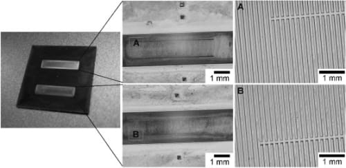
Fig. 8. Photograph and optical images of patterns on parylene-C sample surface imprinted using type D mold under complete filling conditions (T ¼ 270 °C; P ¼ 200 kgf; tH ¼ 900 s).
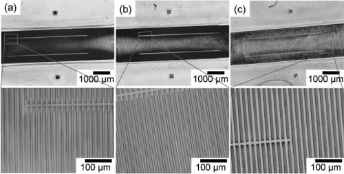
Fig. 9. Micrographs of parylene-C surface (deposited at 45 mTorr) imprinted with the same force of 200 kgf and press hold time of 900 s at different temperatures of (a) 250, (b) 260, and (c) 270 °C. Complete filling was achieved at 270 °C (P ¼ 200 kgf; tH ¼ 900 s).
As previously described in Fig. 2, the crystallinity of a parylene-C film was varied by changing the deposition pressure. Although quantitative analyses were not performed, such a crystallographic change can affect the mechanical, optical and electrical properties of parylene-C, giving rise to the possibility of the fabrication of parylene-C with tailored properties. In this regard, the complete filling conditions for a parylene-C sample deposited at 45 mTorr were also investigated by varying the temperature and using the mold of type C. Figure 9 shows the optical micrographs of the parylene-C surfaces imprinted at different temperatures (250, 260, and 270 °C) with the press force of 2 kN and the press hold time of 900 s. Complete filling could be achieved at the press-head temperature at 270 °C (Tg þ 180 °C).
3.2 Mold cleaning
Mold cleaning is one of the critical issues that need to be addressed to ensure the success of this process. A problem is that most mold release agents (including that used in this study), such as self-assembled monolayers (SAMs), do not provide a sufficient antiadhesion effect under such a high temperature condition as 270 °C. Although the mold could be released without marked destruction of the pattern over the entire imprinted area, the mold surface was contaminated progressively during the repeated imprinting
tests despite the periodic reapplication of the mold release agent. In this case, cleaning is difficult because parylene-C materials are insoluble in all common organic solvents up to 150 °C. It has been reported that parylene-C can be dissolved in Xchloronaphthelene or benzoyl benzoate at temperatures above 150 °C or can be etched by O2 plasma.4) In this study, chloronaphthalene solution and O2 plasma were adopted for mold cleaning. In the initial cleaning process, the contaminated mold was initially cleaned with acetone and DI water in an ultrasonic bath to eliminate the organic contaminations. The mold was then emersed in a chloronaphthalene solution at >175 °C for 3 – 5 h, followed by oxygen plasma etching for 20 – 30 min. Figure 10 shows a typical result of mold cleaning. A clean mold surface could be achieved. Although no data are included, in most cases, a mold could be cleaned sufficiently by emersing in a chloronaphthalene solution at >175 °C for 3 h, followed by oxygen plasma etching for 20 min.
4. Conclusions
In this study, the possible defects (thermal oxidation, delamination, thermal cracking, and insufficient filling) that may occur during parylene-C imprinting were investigated and overcome by tuning the process conditions and mold design. The results are as follows.
- XRD analyses results for the parylene-C films deposited at different pressures (25, 35, 45, and 55 mTorr) indicated that all samples have the same peak at 2θ equal to about 15° and that the crystallinity marked decreased at >45 mTorr.
- By tuning the process conditions and mold design, the patterned fields (composed of arrays of 25-mm-high, 10-mm-wide, and 1-mm-long lines with 10 mm spacing) in 1-mm-thick and 20 mm-sized nickel molds could be successfully replicated onto the 60-mm-thick parylene- C films deposited at both 25 and 45 mTorr. Complete filling over the whole imprint area could be achieved at <270 °C with the press force of 2 kN and the press hold time of 900 s. The designed dummy pattern was effective for achieving complete filling of a patterned field, particularly at the periphery.
- Both thermal cracking and delamination could be prevented even at 270 °C under the established process conditions and mold design with the help of adhesion promotion treatment of silicon substrates (SF6 plasma etching for 2 min and spin-coating of KBM-503-based solution).
- Mold contaminations from parylene-C could be removed by emersing the mold in a chloronaphthalene solution at >175 °C for 3 – 5 h, followed by oxygen plasma etching for 20 – 30 min.
Acknowledgement
This work was supported by Hirose Sensing Technology Co., Ltd. (HST). The authors would like to express their deep gratitude to HST for financial assistance. Also, the authors would like to thank Mr. Akihisa Ueno for his technical support regarding Si micromachining and parylene- C film deposition processes.
References
- Y. Suzuki and Y.-C. Tai: Proc. 16th IEEE Int. Conf. MicroElectro Mechanical Systems (MEMS2003), 2003, p. 486.
- T.-J. Yao, K. Walsh, and Y.-C. Tai: Proc. 15th IEEE. Int. Conf. MicroElectro Mechanical Systems (MEMS2002), 2002, p. 614.
- M. Liger, D. Rodger, and Y.-C. Tai: Proc. 16th IEEE Int. Conf. Micro Electro Mechanical Systems (MEMS ’03), 2003, p. 602.
- E. Meng and Y.-C. Tai: Proc. 18th IEEE Int. Conf. Micro Electro Mechanical Systems (MEMS’05), 2005, p. 568.
- H.-S. Noh, P. J. Hesketh, and G. C. Frye-Mason: J. Microelectromech. Syst. 11 (2002) 718.
- H.-S. Noh, Y. Huang, and P. J. Hesketh: Sensor. Actuators B 102 (2004) 78.
- S. Y. Chou, P. R. Krauss, and P. J. Renstrom: J. Vac. Sci. Technol. B 14 (1996) 4129.
- L. J. Guo: J. Phys. D 37 (2004) R123.
- X.-J. Shen, L.-W. Pan, and L. Lin: Sensor. Actuators A 97– 98 (2002) 428.
- D. Hardt, B. Ganesan, W. Qi, M. Dirckx, and A. Rzepniewski: Innovation in Manufacturing Systems and Technology (IMST), 2004 (https://hdl.handle.net/1721.1/3917).
- H. Becker and C. Gartner: Electrophoresis 21 (2000) 12.
- H. D. Rowland and W. P. King: J. Micromech. Microeng. 14 (2004) 1625.
- H.-C. Scheer and H. Schulz: Microelectron. Eng. 56 (2001) 311.
- H. D. Rowland, A. C. Sun, P. R. Schunk, and W. P. King: J. Micromech. Microeng. 15 (2005) 2414.
- Specialty Coating Systems (SCS): Parylene Conformal Coating Specifications and Properties, (https://www.nbtc.cornell.edu/facilities/ downloads/Parylene%20Information%20Sheets.pdf).
- T. Konishi, H. Kikuta, H. Kawata, and Y. Hirai: Microelectron. Eng. 83 (2006) 869.
- Y. Hirai, T. Yoshikawa, N. Takagi, S. Yoshida, and K. Yamamoto: J. Photopolym. Sci. Technol. 16 (2003) 615.
- Three Bond Co., Ltd.: Threebond Tech. News No. 39 (https:// www.threebond.co.jp/ja/technical/technicalnews/index.html).
- F. Lazzarino, C. Gourgon, P. Schiavone, and C. Perret: J. Vac. Sci. Technol. B 22 (2004) 3318.
- D. W. Grattan and M. Bilz: Stud. Conserv. 36 (1991) 44.
- B. Heidari, I. Maximov, and L. Montelius: J. Vac. Sci. Technol. B 18 (2000) 3557.
- K. Deguchi, N. Takeuchi, and A. Shimizu: Jpn. J. Appl. Phys. 41 (2002) 4178.


