

Article
Related Links
Keisuke Nagato *, Shuntaro Sugimoto, Tetsuya Hamaguchi, Masayuki Nakao
Department of Mechanical Engineering, Graduate School of Engineering, The University of Tokyo, 7-3-1 Hongo, Bunkyo-ku, Tokyo 113-8656, Japan
Abstract
The authors demonstrated an iterative roller imprint method of multilayered nanostructures. A thermoplastic polymer film is imprinted using a nanostructured mold and heated rollers (first layer). The next imprinted thin film is thermally bonded on the backside of the first layer using other rollers. By repeating these processes, a multilayered nanostructure was fabricated. By this method, multilayered nanostructures with an 800 nm pitch line-and-space pattern were fabricated using polymethyl–methacrylate film of 800 nm thickness.
1. Introduction
Electron beam (EB) lithography and ultraviolet photolithography are well-established methods of fabricating two-dimensional (2D) nanostructures on flat surfaces. Recently, nanoimprint lithography (NIL) [1,2] has been increasingly developed as a low-cost fabrication method for replicating 2D nanostructures. NIL can also be used to fabricate three-dimensional (3D, i.e., nonplanar) microor nanostructures such as lens or multistep structures. More importantly, some advanced fabrication technologies for multilayered nanostructures have been proposed and demonstrated, such as repeating nanoimprinting and piling-up steps [3–5]. 3D and multilayered nanostructures are becoming important with the technological advances in nanodevices such as nanoelectromechanical systems [6], nanofluidic devices [7], and nanophotonics [8,9].
In this study, we developed an iterative imprint method using rollers with the aim of fabricating large-area multilayered nanostructures. Roller nanoimprinting has the advantages of pressure uniformity, less force, and high throughput [10–13]. 2D nanostructures are imprinted on a thin polymer sheet, and the imprinted sheet is thermally bonded onto another one. By this method, we demonstrate two different approaches. One of them is multilayered nanogaps advancing the iterative imprint technique, which we have developed [5]. The other is multilayered thin-film nanostructures by a combination of additional deposition process.
2. Thermal roller imprint of 2D nanostructures
There are two different approaches for thermal roller imprint of 2D nanostructures: one is the cylinder mold method, and the other is the sheet mold method [10]. We examined the applicability of the method, we set up both methods. The thermoplastic polymer sheets used are 75-lm-thick polymethyl–methacrylate (PMMA) sheets (Acryplene HBS-005: Mitsubishi Rayon Co., Ltd.). The mold was obtained with electroplated Ni using a master Si substrate with EB resist (ZEP-520A: Zeon Corporation) structures. The structure has a line-and-space pattern with 800 nm pitch and 300 nm depth (Fig. 1a).
In the cylinder mold method, the cylinder mold was made by bending the Ni mold (thickness: 100 lm) and welding their ends. This mold is set up on a roller covered by a sheet heater (roller diameter: 80 mm, width: 90 mm). The whole mold surface was heated through imprinting and demolded (illustration in Fig. 1b). On the other hand, in the sheet mold method, the sheet mold was also fabricated to round shape for continuous replication, and a smaller roll heater was integrated. In other words, the PMMA sheet is fed with the sheet mold, imprinted by the backup roll heater, cooled together with the sheet mold after passing the roll heater, and subsequently demolded (illustration in Fig. 1c).
In the both methods, the pressure was applied from the backside of the PMMA sheet using a backup roller covered with silicone rubber. The rollers are driven synchronously by a motor. The feeding speed, imprinting temperature, and imprinting pressure were 10 mm/s, 145 °C, and 1 MPa, respectively. The imprinting temperature was measured using a thermocouple welded on the Ni mold surface. The imprinting pressure was measured using pressure sensor sheets (Prescale LLW, 4LW: Fujifilm Corp.). This imprint pressure is lower than general nanoimprint lithography. This is because the uneven pressure is improved by the silicone–rubber backup roller and line contact of the roller pressing.
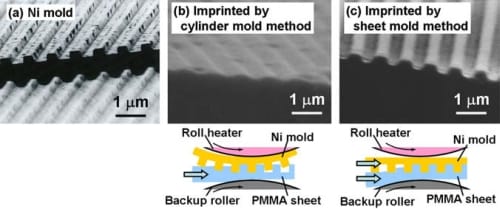
Fig. 1. SEM images of cross sections of (a) Ni mold (800 nm period line-and-space, 300 nm depth), PMMA surfaces which are (b) imprinted by hot cylinder mold and immediately demolded, and (c) imprinted by sheet mold with a backup roll heater and demolded after cooled together with the sheet mold. (For interpretation to colours in this figure, the reader is referred to the web version of this paper.)
Fig. 1 shows the scanning electron microscopy (SEM, S-4000, Hitachi) images of cross sections of the PMMA films imprinted with (b) the cylinder mold and (c) the sheet mold. The structures obtained with the cylinder mold have only 40 nm depth and those obtained with the sheet mold have 300 nm depth. In the cylinder mold experiment, the imprinted and demolded surface structures were reflowed by the hot mold. On the other hand, in the sheet mold experiment, the imprinted structures were cooled together with the Ni mold under the glass transition temperature (Tg, 120 °C). Accordingly, we used the sheet mold method for the subsequent experiments on multilayered nanostructures.
3. Experiment on iterative roller imprint of multilayered nanostructures
We demonstrated two methods: forming gaps (made of air or vacuum) between PMMA thin nanostructures (Fig. 2a) and filling another thin material in each of the PMMA nanostructures (Fig. 2b). The basic process of the former is the same as that described in our previous work [5]. The future schematics of the systems are shown in Fig. 3. In the latter, the imprinted nanostructure is deposited using another material, and then another sheet is fed, imprinted, and bonded at the same time.

Fig. 2. Process flows for (a) multilayered nanogaps and (b) multilayered thin-film materials by additional deposition. (For interpretation to colours in this figure, the reader is referred to the web version of this paper.)
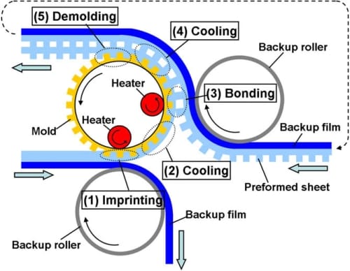
Fig. 3. Schematic of roller imprint system for multilayered nanostructures. (For interpretation to colours in this figure, the reader is referred to the web version of this paper.)
The experimental details of the multilayered nanogap structures are described as follows. The roller mold described in Section 2
was used. The thin PMMA film (thickness: 800 nm) was obtained by spin-coating. The PMMA solution in toluene is spincoated on Cr film sputtered on a Si wafer and covered by a lubricant (Durasurf HD-2101Z: Daikin Chemical). This PMMA film is transferred to a silicone rubber film, which corresponds to the backup film in Fig. 3. The PMMA film is imprinted using the Ni roller mold and a backup silicone roller together with the backup film. The feeding speed, imprinting temperature, and imprinting pressure were 10 mm/s, 145 °C, and 1 MPa, respectively. After the imprinting and cooling to 100 °C, the backup silicone film is peeled off from the PMMA thin film. Next, a preformed PMMA thin film with backup film is fed on the back of the PMMA thin film stacked in the roller mold. They are pressed using another backup roller and thermally bonded with a roll heater. The heater temperature was approximately 100 °C and the bonding pressure was 0.1 MPa.
For the multilayered thin-film nanostructures, the first layer is imprinted under the same condition as the nanogap nanostructures. The nanostructured PMMA thin film on a backup film is sputtered with Cr. The deposited PMMA is pressed together with another 800-nm-thick PMMA film using the Ni roller mold and a backup roller. The second layer was imprinted and its back side was bonded on the Cr nanostructure on the first PMMA film. The heater temperature and bonding pressure were 130 °C and 1 MPa, respectively. Wedemonstrated the fabrication of multilayered Cr thin-film nanostructures by rotating the film by 90° in each imprinting step.
4. Results and discussion
4.1. Iterative roller imprint for nanogap structures
We verified the PMMA surface temperature for bonding with keeping the nanogaps. Fig. 4 shows the SEM images of the cross sections of the multilayered nanogaps. When the nanostructured PMMA sheet was bonded on the preformed sheet at 100 °C at the feeding speed of 10 mm/s, the nanogaps were not lost, as shown in Fig. 4a. However, when the sheets were bonded at 105 °C, the nanogaps became smaller as shown in Fig. 4b. When the bonding temperature was over 110 °C, the nanogaps became completely filled and disappeared. Furthermore, we also demonstrated bonding five-layered nanogaps with the bonding temperature of 100 °C (Fig. 4c). The nanogaps formed at the former bonding step (lower layer) became smaller in size. This is because the lower layer was exposed to heat longer. With higher-speed feeding of the sheets, i.e., shorter-time exposure to heat, the nanogaps may be maintained the initial size (400 nm width and 300 nm height).
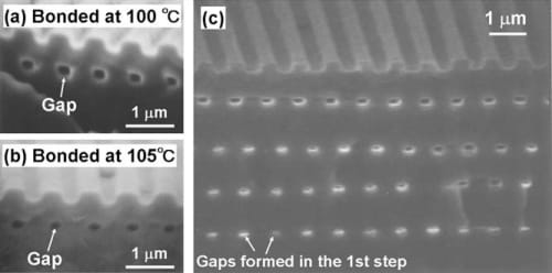
Fig. 4. SEM images of cross sections of multilayered nanostructures fabricated with process flow of Fig. 3a. (a) Nanogaps formed by bonding at 100 °C, (b) nanogaps formed by bonding at 105 °C, and (c) multilayered nanogaps with five-layered nanostructures.
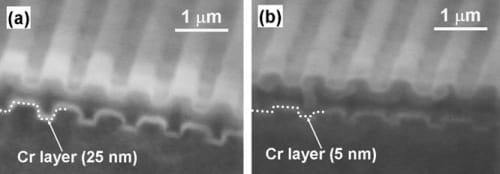
Fig. 5. SEM images of cross sections of multilayered nanostructures fabricated with process flow of Fig. 3b. (a) Cr film nanostructures with thickness of 25 nm and (b) thickness of 5 nm.
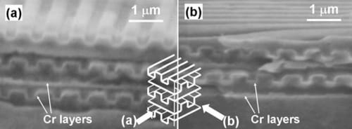
Fig. 6. SEM images of cross sections of five-layered Cr film nanostructures fabricated by rotating 90° before each imprinting step.
4.2. Iterative roller imprint for multilayered thin-film nanostructures
Multilayered thin-film nanostructures were fabricated by the iterative roller imprint method. As shown in Fig. 2b, thin films deposited on polymer surfaces that are thermally imprinted were piled up. Fig. 5a and b shows the results of the imprintedPMMAthin film on the nanostructured surface of Cr film is sputtered on a preformed first layer with thicknesses of 25 and 5 nm, respectively. Although the nanostructure of the 25-nm-thick Cr film was maintained, that of the 5-nm-thick film was deformed by the roller pressing during the thermal imprinting of the second layer. Furthermore, we demonstrated five-layered Cr thin-film nanostructures. In the experiment, the sheet was rotated 90° in each imprinting step. Fig. 6a and b shows the cross-sectional SEM images (at two different angles) of the multilayered thin-film nanostructures. Materials other than Cr can be used for deposition, and those in other thicknesses can also be used. When designing with other materials, the change in the form of the deposited materials caused by the imprinting pressure should be verified. The combination of imprinting of polymer and depositing of other materials can be one of the candidate fabrication methods for multilayered nanostructures.
5. Conclusions
We have developed an iterative roller imprint method of multilayered nanostructures. Our experiment demonstrated two different multilayered nanostructures: nanogaps by repeating imprinting and bonding sheets and thin-film nanostructures by repeating imprinting polymer films and depositing other material. The nanogap pattern with a pitch of 800 nm and a depth of 300 nm was multilayered using PMMA. By the combination of Cr sputtering with imprinting polymer films, the thin-film nanostructures were also demonstrated. This iterative roller imprint method will lead to the low-cost mass production of multilayered nanostructures.
Acknowledgments
The master substrate for the electroplated Ni mold was fabricated using the EB writer (F5112+VD01) at the University of Tokyo VDSI Design and Education Center (VDEC), which was donated by Advantest Corporation. This work is partially supported by a Grant-in-Aid for Scientific Research (S) (No. 080300000166) and by the Global Center of Excellence (G-COE) Program ‘‘Global Center of Excellence for Mechanical Systems Innovation (GMSI)”, from the Ministry of Education, Culture, Sports, Science and Technology, Japan.
References
- S.Y. Chou, P.R. Krauss, P.J. Renstrom, Appl. Phys. Lett. 67 (1995) 3114.
- H. Schift, J. Vac. Sci. Technol. B 26 (2008) 458.
- L.–R. Bao, X. Cheng, X.D. Huang, L.J. Guo, S.W. Pang, A.F. Lee, J. Vac. Sci. Technol. B 20 (2002) 2881.
- M. Nakajima, T. Yoshikawa, K. Sogo, Y. Hirai, Microelectron. Eng. 83 (2006) 876.
- H. Suzuki, K. Nagato, S. Sugimoto, K. Tsuchiya, T. Hamaguchi, M. Nakao, J. Vac. Sci. Technol. B 26 (2008) 1753.
- H.G. Craighead, Science 290 (2000) 1532.
- H. Wu, T.W. Odom, D.T. Chiu, G.M. Whitesides, J. Am. Chem. Soc. 125 (2003) 554.
- Y.A. Vlasov, X.-Z. Bo, J.C. Sturm, D.J. Norris, Nature 414 (2001) 289.
- T. Hamaguchi, H. Yonemoto, K. Nagato, K. Tsuchiya, M. Nakao, J. Vac. Sci. Technol. B 26 (2008) 1771.
- H. Tan, A. Gilbertson, S.Y. Chou, J. Vac. Sci. Technol. B 16 (1998) 3926.
- S.-W. Youn, M. Ogiwara, H. Goto, M. Takahashi, R. Maeda, J. Mater. Process. Technol. 202 (2008) 76.
- S.H. Ahn, L.J. Guo, Adv. Mater. 20 (2008) 2044.
- M. Ogino, M. Hasegawa, A. Miyauchi, in: The first Asian Symposium on Nano Imprint Lithography (ASNIL 2008), p. 37.
![]()