


A replication process of metallic micro-mold by using parylene embossing and electroplating
Sung-Won Youn a,*, Hiroshi Gotoa, Masaharu Takahashia, Shoji Oyama b,1, Yasuhiko Oshinomi b,1, Kinya Matsutani b,1, Ryutaro Maeda a
a Advanced Manufacturing Research Institute, National Institute of Advanced Industrial Science and Technology (AIST), 1-2-1 Namiki, Tsukuba, Ibaraki 305-8564, Japan
b Design Engineering Group, Engineering Department, Hirose Sensing Technology (HST) Co. Ltd., Kaneko No. 2 Building 8F, 2-6-23, Shinyokohama, Kohoku-ku, Yokohama-shi, Kanagawa 222-0033, Japan
Abstract
This study demonstrated a replication process for metallic micro-mold that combines the parylene-C (poly-chloro-p-xylylene C) hotembossing and electroplating techniques. A nickel original master was fabricated using the deep RIE silicon etching followed by the electroplating process. Then, the patterned fields composed of arrays of 25 lm-high, 10 lm-wide and 1 mm-long lines with 10 lm spacing in nickel molds were successfully replicated on the 60 lm-thick parylene-C films by the hot-emboss process. Under complete filling conditions, the deviation of the replicated micropattern was less than 2.4%. The electroplated copper successfully filled parylene-C replica master patterns with the aspect ratio of 2.5 without the void formation by both adding organic addictives and controlling the seed layer thickness. After electroplating, the copper micro-mold could be successfully separated from the parylene-C replica master. © 2007 Elsevier B.V. All rights reserved.
Keywords: Metallic micro-mold; Hot-embossing; Lithography; Parylene-C (poly-chloro-p-xylylene C)
1. Introduction
For decades, hot-embossing (or thermal nanoimprint lithography) techniques have been utilized extensively for the definition of nano/micro-features with a high throughput at a low cost [18]. Recently, hot-embossing techniques have been applied not only to the formation of micropattern but also to the high volume production of microdevices such as micro-reactors [2], micro-fluidic systems [9] and micro-optical devices (e.g., diffraction gratings, waveguides, micro-ring resonators and MachZehnder interferometers) [10,11]. Furthermore, several kinds of large area processing methods such as the step-and-stamp [3], rolling [12] and flat-large mold [4,13] embossing techniques are being actively studied for the further progress of hot-embossing technologies. Nevertheless, there still remain other critical issues that need to be more studied for the acceptance of hot-embossing technologies in industrial applications. One of them is the relatively high cost for mold fabrication. Here, we were especially interested in low-cost processes for the fabrication of metallic molds. Generally, fabrications of metallic micro-molds are performed by the well-developed silicon micromachining process (which allows for the fabrication of high-precision microstructures by means of anisotropic etching, reactive ion etching and deposition) and a subsequent metal electroplating. The cost for silicon micromachining is relatively high and occupies a great portion of entire cost for metallic mold fabrication. Further, a silicon master cannot be reused as it is removed by a KOH etching after electroplating. Our experiences have shown that generally used micromolds (e.g, silicon, silicon oxide and metal molds) did not last long in mass production because of the decrease of mold quality (e.g., warping, distortion, deformation or cracking of the mold). Such mold defects can be easily generated during hot-embossing due to the various factors such as the unevenness in the sample/mold thickness, the small and hard dust particles, the pattern geometries, the inadequate embossing/demolding conditions and others [4,14]. This aspect implies that larger mold surface has higher possibility of shorter mold life as well as higher production cost.
For the development of the simple, low-cost and efficient process for the fabrication of multiple masters, various combinations of metal and polymer replication processes have been explored and suggested [1517]. Among those techniques, an electroforming process using a replicated polymethylmethacrylate (PMMA) or polycarbonate (PC) master is one of the most common processes because polymers can be easily patterned by hot-embossing [16,17]. Parylene- C (poly-chloro-p-xylylene C) with a wide range of applications (e.g., microvlaves, DNA separation/ detection channels, gas chromatographic column, shear stress sensors, and microspeakers and others) is also one of the promising candidates as a master material due to its compatibility with traditional micro fabrication technology and its superior properties such as stress-free conformal deposition, high mechanical flexibility (about 4 GPa of elastic modulus), low defect density, large linear-elastic range (yield strain up to 3%), excellent chemical inertness and biocompatibility [1823]. Moreover, electroplate metallic mold can be easily removed from parylene-C master since the adhesion between parylene-C and most substrates (e.g., metals and silicon) is generally poor due to the hydrophobic nature of parylene-C film. In this regard, a metal electroforming process using a patterned parylene- C master is a very good combination for the metallic mold replication. The sub-micro scale processing of parylene-C includes direct deposition with/without a sacrificial layer [19], dry etching (plasma, RIE and DRIE) [21] and micromolding [22,23]. Wet etching techniques cannot be used for this purpose because parylene is inert to most chemicals at room temperature [21]. To our knowledge, hot-emboss technologies have not been used for microstructuring parylene- C.
In this study, we demonstrate a replication process for metallic micro-mold that combines the parylene-C embossing and electroplating techniques. The aims of this study are the fabrication of the micro-patterned parylene-C master by a hot-emboss process and its application to the metallic mold replication. The detailed process is described in the next section.
2. Process layout
The scheme utilized in this work is detailed in Fig. 1. The process began with the deposition of a parylene film on silicon substrate. The ability for conformal deposition is one of reasons for the use of this material because it enables the formation of stress-free and extremely thin films with well controlled thickness. The film thickness is one of major factors that strongly affect the flow rate of material during embossing [4]. For the second step, a hot-embossing technique is employed for parylene microstructuring as it is a simpler and faster process than other parylene micro structuring methods, such as direct deposition with/without a sacrificial layer, dry etching and micromolding. Nickel mold for hot-embossing was prepared by a silicon micromachining process and a damascene process. After hot-embossing, thin conductive layers of Ta/Cu were sputtered on the embossed parylene surface to define a barrier layer and a seed layer for the electroplating. No adhesion promoter such as the dilute solution of organic silane and the oxygen plasma is used for the easy separation between the parylene and the metallic mold. Subsequently, a metal is electroplated to sufficient thickness. In the final step, a metal mold is separated from the parylene manually.
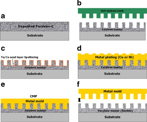
Fig. 1. Process layout for replicating metallic micro mold by using parylene-C embossing and electroplating techniques. (a) Parlyene deposition, (b) hot-embossing, (c) sputtering of seed layers, (d) electroplating, (e) planarization and (f) separation.
3. Experimental details
Parylene-C (poly-chloro-p-xylylene, diX-C, Daisankasei Co. Ltd., Japan) used as an emboss material is a linear crystalline thermoplastic polymer of which the glass transition temperature is less than 90 °C and the melting temperature is 290 °C. Parylene-C films with a thickness of about 60 lm were deposited at room temperature on silicon wafers by a vapor deposition polymerization method using a PDS2010 Labcoater (Specialty Coating Systems, USA). The parylene coated Si wafers were then cut to 15 · 15 mm2 by dicing. To improve the adhesion of a parylene onto silicon, 4-in. silicon wafers were etched using a SF6 plasma for 2 min, and spin-coated with an IPA:distilled H2O:KBM-503 100:100:1 solution before parylene deposition. Embossing tests were performed in a hotemboss equipment, which is designed to emboss 3 · 3 cm2 samples. The maximum embossing temperature was 700 °C, and the maximum press force was 2 kN. A pumping system allows embossing samples under vacuum, with a pressure of 1 Pa inside the chamber. In the first step of hotembossing process, the mold was pressed into a parylene film at a temperature well above the glass transition temperature (Tg) of the parylene, where the parylene has relatively low viscosity and can flow under applied pressure. The pressing pressure then held for a sufficient time to achieve complete filling. This hold time is a function of both material temperature and pressing force [8]. After natural cooling to 80 °C (below Tg) the applied force was released and the nickel mold was removed from the parylene sample. Natural cooling was adapted since too fast cooling rate can cause cracking and delamination of parylene film after cooling due to the large difference in the coefficient of thermal expansion between the silicon and parylene. Prior to hot-emboss tests, local flatness distortions in the mold and/or sample was evaluated using a pressure-sensitive film (Prescale film, Fuji-Film Co., Japan), and compensated by using spacers. A GC-1720 (Sumitomo 3M, Japan) solution was used as a mold release agent. A chloronaphthalene solution (heated at >175 °C) and an oxygen plasma were used as mold cleaning agents. Thin metal layers of Ta/Cu were sputtered on the embossed parylene samples as conductive and conformal seed layers for electroplating copper. A profile meter (Talysurf S4C, Taylor Hobson), an interferometric surface profiler (Zygo New View 5000) and a scanning electron microscopy (SEM) were used to obtain the morphological data of the processed samples.
4. Results and discussion
The silicon master structure for mold was prepared by a silicon micromachining process such as deep reactive ion etching (DRIE). The channel width was fixed at 10 μm and the depth was fixed at 25 lm by the standard Bosch etching cycles to achieve the aspect ratio of 2.5. The nickel mold with the size of 20 · 20 mm2 and the thickness of 0.3 mm was fabricated by the subsequent electroplating process and by KOH etching of silicon master.

Fig. 2. Photograph and optical micrographs of nickel mold.
Figs. 2 and 3 show the photograph, optical micrographs and scanning electron microscopy (SEM) images of nickel mold that was fabricated using the deep RIE silicon etching followed by the electroplating process. The nickel mold is 20 · 20 mm2 in size and has arrays of 25 μm-high, 10 μm-wide and 1 mm-long lines with 10 lm spacing on its surface as known from the analysis results of optical interferometry (Fig. 4). The mean height and surface roughness of Ra for the replicated micropatterns were 25.4 μm and 131 nm, respectively. The thickness of the mold was 0.3 mm that is thinner than generally used metallic molds. In general, a thinner mold provides better conformal contact with a sample surface and reduces the pressure needed for the complete filling during the embossing step since it is more flexible (or deformable) than thicker one [2].
For the hot-embossing tests, the pinhole-free parylene-C film with thicknesses of about 60 lm was confirmly deposited on the silicon sample at room temperature. The thickness of a parylene film was set above twice of the master structure height (of mold) to achieve easy relaxation of localized strain for the fast materials flow [24]. The film thickness could be tuned by varying the quantity of a dimmer and the deposition time.

Fig. 3. SEM images of arrays of 25 lm-high, 10 lm-wide and 1 mm-long lines with 10 lm spacing in nickel mold: (a) periphery; (b) middle; (c) a magnification image of (b).

Fig. 4. 3D image and surface profile of the nickel mold surface measured using optical interferometer.
For the success of parylene-C embossing, the vacuum environment, the subtle tuning of process parameters (temperature, pressure and time) and the fabrication of well-designed mold are crucial. Vacuum environment is critical to prevent the air entrapment and the oxidative degradation of parylene which can happen above 120 °C in air [23]. It is generally known that a good replication result can be acquired when the embossing temperature is set to be higher than the flow temperature (Tf) of the polymer because the modulus and viscosity are remarkably reduced above Tf. In the viscous liquid flow state regime (>Tf), the motion of entire chains takes place and the polymer flows by chain sliding and the deformation is irreversible, which makes it the right temperature range for embossing [2]. It was also reported that an optimal imprinting temperature is generally found 7080 °C above the Tg of the material used [2]. Contrarily, for embossing parylene-C, embossing temperature needs to be set much higher than that of general emboss materials because the Tf of parylene is about 230 °C (Tg + 140 °C) [25]. From the preliminary study, a series of hot-emboss tests using parylene samples were carried by varying the maximum heating temperature under the same cooling, force and press hold-time to investigate the complete filling conditions. It was found that the parylene- C is very hard to be deformed even over its glass transition temperature (Tg = 100 ° C) and was also found that the temperature is a more dominating factor than pressure and time.
Figs. 5 and 6 show the photograph, optical micrographs and SEM images of the micropatterns on parylene surfaces hot-embossed under the full filling conditions. After hotembossing, a thin conductive layer of Ta/Cu was sputtered on the embossed parylene surface to define a seed layer for the electroplating. Another role of conductive layers is to prevent charge-up phenomena [19] during SEM observation since a parylene is a good insulator. Complete filling could be obtained at press-head temperature about 270 °C (Tg + 180 °C) with the press force at 2 kN and the press hold-time of 900 s without the deformation of nickel mold (a emboss velocity at 0.3 mm/min and a heating rate at 0.5 °C/s). The contamination of mold surface could be removed by dipping in a chloronaphthalene solution at >175 °C for 3 h, and the subsequent oxygen plasma etching for 20 min. As shown in the photograph (Fig. 5), the delamination of parylene film did not occur since good adhesion between the deposited parylene films and the silicon wafers could be achieved by an adhesion promotion treatment (for details see Section 3) prior to deposition. The optical micrographs and SEM represented that the features from the nickel mold are very well reproduced with good pattern fidelity over the whole parylene-C sample surface. In Fig. 7, the surface profile of the embossed sample surface was investigated using an optical interferometer. The mean height and surface roughness of Ra for the replicated micropatterns were 24.9 μm and 237 nm, respectively. The parylene microstructure left on the substrate after hot-embossing can also be used as the component of micro-devices itself.

Fig. 5. Photograph and optical micrographs of parylene/silicon sample hot-embosed at 270 °C with the force of 2 kN and the press hold-time of 900 s.

Fig. 6. SEM images of parylene/silicon sample hot-embosed at 270 °C with the force of 2 kN and the press hold-time of 900 s.

Fig. 7. 3D image and surface profile of the hot-embossed Parylene-C sample measured using optical interferometer
For copper electroplating, a parylene-C sample was prepared by hot-embossing under complete filling conditions. Tantalum and copper were employed as a barrier layer and seed layer, respectively, and the copper was then electroplated to sufficient thickness. As can be observed from cross-sectional SEM (Fig. 8), the electroplated copper successfully filled patterns with the aspect ratio of 2.5. Voidfree filling of high aspect ratio trenches during electroplating depends on a complex set of parameters, and fillingdefects leading to voiding may occur if the bath additive concentrations are not correct for the target pattern structure, or if the seed layer is too thin on the sidewalls or too thick near the trench opening [26]. The void formation during copper electroplating could be solved using organic addictives and by the control of the seed layer thickness (Fig. 8 (c)). Removing seed layers from the tops of the pattern structures may also be solution to avoid void formation [27]. Although the copper micro-mold was replicated as an example in this study, other common electroplating metals such as nickel and Au can also be used.

Fig. 8. Cross-section SEM images of hot-embossed parylene-C after copper electroplating. Hot-embossed parylene-C surfaces were sputtered with the barrier layer of 25 nm-thick Ta and the seed layers of (a) 100 nm-thick Cu, (b) 200 nm-thick Cu and (c) 400 nm-thick Cu.

Fig. 9. SEM images of replicated copper micro-mold; (a) shows the backside of electroplated copper before chemical mechanical polishing.

Fig. 10. SEM images of parylene-C master surface after copper removal.
After copper electroplating, the copper micro-mold could be separated from the parylene sample manually since a no pre-treatment of the embossed parylene-C surface was performed as shown in Fig. 9. Commonly, the surface of parylene is pre-treated with oxygen plasma to enhance the adhesion between parylene and metallic seed layers as its adhesion to most materials is usually very poor. The SEM images of parylene master structures after copper removal are shown in Fig. 10. No noticeable defects, such as deformation and cracking, in the parylene master occurred due to its large-elastic range. Although a parylene master can be reused several times, its reusability strongly depends on its aspect ratio and cleanness. The anti-adhesion treatment of mold surfaces is one of critical issues that need to be addressed for the further progress of this process. A problem is that most mold release agents such as self-assembled monolayers (SAMs) do not provide sufficient anti-adhesion effect under such high temperature condition. Although releasing the mold could be done without remarkable destruction of the pattern in the entire imprinted area, the mold surface was contaminated progressively during the repetitive hot-embossing tests despite the periodic reapplication of the mold release agent. This deficiency increase the process cycle time remarkably because the removal of parylene-C contamination from nickel mold can be accomplished only by a time-consuming process, i.e, cleaning using a chloronaphthalene solution (heated at >175 °C) and an oxygen plasma. A fluorinated diamond-like carbon (F-DLC) coating on a mold surface may be one solution [28], but further study is needed because the adhesion of DLC films onto nickel is generally poor.
5. Conclusions
In conclusion, the replication process that combines the parylene-C embossing and electroplating techniques was effective to replicate metallic micro-molds. The patterned fields composed of arrays of 25 lm-high, 10 lm-wide and 1 mm-long lines with 10 μm spacing in nickel molds were successfully replicated on the 60 lm-thick parylene-C films by hot-embossing at 270 °C with the press force at 2 kN and the press hold-time of 900 s without the deformation of nickel mold. Under given conditions, the deviation of the replicated micropattern was less than 2.4% and the surface roughness of the replicated patterns was 237 nm. The electroplated copper successfully filled parylene-C replica master patterns with the aspect ratio of 2.5 by adding organic addictives and by controlling the seed layer thickness. The geometrical dimensions measured throughout process showed no observable dimensional changes. The technique can be applied to the low-cost mass production of metallic components in micro-devices as well as metallic micro-molds. Additionally, integrating copper with lowdielectric constant film (such as parylene) by using hotembossing and electroplating is a promising method to interconnect small geometry integrated circuits (ICs) if research regarding the adhesion improvement between the parylene-C and the electroplated copper are sufficiently carried out.
Acknowledgements
The authors express their deep gratitude to the HST Co. Ltd. (Hirose Sensing Technology Co. Ltd.) for financial assistance. Also, the authors thank Mr. Akihisa Ueno for his technical support regarding Si micromachining and parylene-C film deposition processes.
References
- S.Y. Chou, P.R. Krauss, P.J. Renstrom, J. Vac. Sci. Technol. B 14 (6) (1996) 4129.
- L.J. Guo, J. Phys. D Appl. Phys. 37 (2005) R123.
- C.M.S. Torres, S. Zankovych, J. Seekamp, A.P. Kam, C.C. Cedeno, T. Hoffmann, J. Ahopelto, F. Reuther, K. Pfeiffer, G. Bleidiessel, G. Gruetzner, M.V. Maximov, B. Heidari, Mater. Sci. Eng. C 23 (2003) 23.
- H.-C. Scheer, H. Schulz, Microelectron. Eng. 56 (2001) 311.
- X.-J. Shen, L.-W. Pan, L. Lin, Sensor. Actuat. A 9798 (2002) 428.
- H.D. Rowland, W.P. King, J. Micromech. Microeng. 14 (2004) 1625.
- V.C. Sunder, H.-J. Eisler, T. Deng, Y. Chan, E.L. Thomas, M.G. Bawendi, Adv. Mater. 16 (23-24) (2004) 2137.
- D. Hardt, B. Ganesan, W. Qi, M. Dirckx, A. Rzepniewski, in:
Innovation in Manufacturing Systems and Technology (IMST) 2004,
- J. Narasimhan, I. Papautsky, J. Micromech. Microeng. 14 (2004) 96.
- M.T. Gale, C. Gimkiewicz, S. Obi, M. Schnieper, J. Sochtig, H. Thiele, S. Westenhofer, Opt. Laser. Eng. 43 (2005) 373.
- C.-G. Choi, S.-P. Han, M.-Y. Jeong, Opt. Commun. 235 (2004) 69.
- H. Tan, A. Gilbertson, S.Y. Chou, J. Vac. Sci. Technol. B 16 (6) (1998) 3926.
- B. Heidari, I. Maximov, L. Montelius, J. Vac. Sci. Technol. B 18 (6) (2000) 3557.
- Mastering Technology, Magazine of Optical Disk Systems, July
August 1998.
. - C.Y. Chang, S.Y. Yang, J.L. Sheh, Microsyst. Technol. 12 (2006) 754.
- H. Li, J. Lin, R. Su, Z.W. Cai, K. Uchiyama, Electrophoresis 26 (2005) 1825.
- K. Deguchi, N. Takeuchi, A. Shimizu, Jpn. J. Appl. Phys. 41 (2002) 4178.
- Y. Suzuki, Y.-C. Tai, in: Presented at the 16th IEEE Int. Conf. on MicroElectroMechanical Systems (MEMS2003), Kyoto, Japan, January 1923, 2003, p. 486.
- T.-J. Yao, K. Walsh, Y.-C. Tai, in: Presented at the 15th IEEE. Int. Conf. on MEMS (MEMS2002), Las Vegas, Nevada, USA, January 2024, 2002, p. 614.
- M. Liger, D. Rodger, Y.-C. Tai, in: Presented at the 16th IEEE Int. Conf. on Micro Electro Mechanical Systems (MEMS 03), Kyoto, Japan, January 1923, 2003, p. 602.
- E. Meng, Y.-C. Tai, in: Presented at the 18th IEEE Int. Conf. on Micro Electro Mechanical Systems (MEMS05), Miami, USA, January 30February 3, 2005, p. 568.
- H.-S. Noh, P.J. Hesketh, G.C. Frye-Mason, J. Microelectromech. Syst. 11 (6) (2002) 718.
- H.-S. Noh, Y. Huang, P.J. Hesketha, Sensor. Actuat. B 102 (2004) 78.
- H.D. Rowland, A.C. Sun, P. Randy Schunk, W.P. King, J. Micromech. Microeng. 15 (2005) 2414.
- Three Bond Co. Ltd., Parylene Coating System, Threebond Technical
News. 39, 1.
- J. Tower, M. Gostein, K. Otsubo, A. Kawasaki, Future Fab Int. 15
(2003).
- C.R. Keppeler, D.A. Dornfeld, Micromilling for Mold Fabrication,
2003,
- K. Nakamatsu, N. Yamada, K. Kanda, Y. Haruyama, S. Matsui, Jpn. J. Appl. Phys. 45 (35) (2006) L954.
